
The semiconductor shortage has shone a spotlight on the fragility of the semiconductor and how quickly supply of key parts can dry up. Though the threat of recession implies that shortage situation is set to go into reverse, the news for future users of advanced silicon is not necessarily good. Chipmakers are finding it increasingly hard to offer the same scaling-driven cost reductions they did in the past and the growing complexity of what they make will likely make it more expensive to deploy additional capacity when demand spikes.
The good news is that, otherwise, silicon scaling is in decent health according to the latest projections from the IEEE’s International Roadmap for Devices and Systems (IRDS) group. And the industry has found a way to keep a lid on costs in the shorter term.
Extreme ultraviolet (EUV) lithography has done a great deal for chipmaking costs, Paolo Gargini, IRDS chairman and Intel fellow, explained at the May readout session for the roadmap.
Since 2018, the number of EUV tools in production has more than doubled and sales of 193nm immersion equipment have fallen, despite a tick up in capital expenditure in response to the chip shortage.
Individual EUV machines cost more than their predecessors but only require one pass to expose a single, high-precision layer on the wafer surface. By now, 193nm immersion would have required four exposures and, to maintain throughput, as many machines in the fab. Gargini pointed out that even taking the cost differential into account, EUV works out approximately half the cost.
EUV, however, is quickly reaching the point where it too may need multiple exposures to define the features for a layer, which will push more cost into the process. In order to meet the aggressive scaling requirements for the low-level metal interconnect layers in the post-3nm nodes, the minimum feature size that a tool has to be able to define reduces below 20nm: not much longer than the 13nm wavelength delivered by the laser source.
One option that ASML is pursuing aggressively is a switch to EUV tools that work with a higher numerical aperture (NA) to squeeze out a little more resolution: with the ability to handle features that are approximately 40 per cent smaller. The Dutch company is working on having the first of these tools ready by the end of 2025, in time for a second wave of 2nm-node products, which will likely sport 20nm metal spacing.
The AI-focused systems companies who want the largest chips may have to settle for multiple patterning of one stripe or another. Harry Levinson, principal lithographer at HJL Lithography, explained at the International Symposium on Roadmapping Devices and Systems that the size of the field that a tool can expose at once halves compared to the current EUV generation. "We either have to expose half the chip at a time and stitch it together or find alternative solutions," he said.
Simulations performed by Imec and Synopsys have suggested that high-NA combined with stitching will produce better-resolved images on the die compared to the kind of double patterning employed with 193nm immersion.
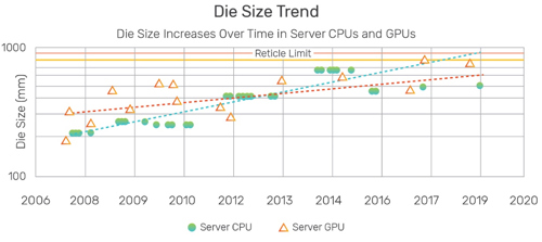
The reduction in throughput with its corollary in production costs comes on top of other factors. The need to make interconnect layers with high aspect ratios to reduce resistance, deal with stacked nanosheets in tall transistors and introduce new transistor-channel and interconnect materials are all likely to increase manufacturing costs, on top of the cost that comes with the cut in effective throughput for big monolithic chips that will come from changes made to EUV lithography.
Die yields
The combination of complexity and die size is placing an even greater focus on die yield.
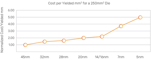
"The cost per yielded millimetre square is changing the cost efficiency because of yield losses due to process complexity and also due to [the trend in] die size increasing across node generations," says Mustafa Badaroglu, principal engineer at Qualcomm and chair of the IRDS More Moore group, which focuses on IC-process scaling.
Yield management has historically been a process of keeping stray dust particles out of the reaction chambers and other equipment as the wafers make their way through the fab. Though failures in certain types of products will certainly focus attention on their production defects, yield optimisation has proceeded mostly without input from design. That is changing. Part of the reason is that in some feature sizes are so small that the stray particles that cause failures may be the chemical agents needed for the processes themselves. They can produce kinks in the edges of gates or metals or form clumps, leading to unwanted defects in the surfaces of the thin films that separate parts of a transistor or cause gaps and voids in vias.
"Five to ten years ago, the yield team really had the capabilities to stay ahead of the quality and requirements that the device side needed for maintaining proper yields," says Dan Wilcox, director of process engineering at Page Southerland Page and co-chair IRDS yield group. But, he adds, the mechanisms that control yield have become more complex and difficult to track. At the same time, some defects are far more important than others. To try to understand them, the yield group started to work more closely with Badaroglu’s more design-focused group.
"We're collaborating with Mustafa almost weekly to understand things in the details of the device like the gate stack, the metallisation and the contact modules...Those risk areas can then end up being defined by a tool or a process or a material that's used. It's now more like a sniper versus a shotgun approach in trying to control these defects and improve yield," Wilcox adds.
Another important change is the nature of yield failures. Traditionally, if a chip did not make it through the test process, that was a yield failure. Today, the concern is shifting towards resilience and reliability. Badaroglu says many of the bigger devices are going into automotive and server applications that are expected to run 24/7 and which may need to survive higher operating temperatures than their smaller counterparts in personal computers and mobile devices.
Chips with problems may not be apparent until they are running in the system and suddenly start to prove unreliable because imperfections lead to connections shorting or breaking. One kinds of mechanism that troubles the yield managers is bias temperature instability: as a transistor ages it traps more and more charges on the gate up to the point where it fails to switch. The carriers tend to accumulate at defects. The high-k dielectrics that are now fundamental to forming gate stacks tend to create more of these interface traps. At the same time, as gates scale down, it is harder to take advantage of the averaging effect over the full gate area. Models produced by the more-Moore group are now helping the yield team on the IRDS work out which parts of the manufacturing process need the most work. They have found ensuring the gate surface is as clean as possible is one of the ways of reducing the risk of bias instability surfacing.
"We've gone from reactive to predictive. And now what we're really calling it is prescriptive. We're doing that by using a multitude of different collaborations, sharing that information, taking things that we're learning from these groups and applying it to experiments," says Wilcox, ultimately turning the information into recommendations for the purity standards for materials and how they are used in the fab.
Though chip sizes and lifetime expectations have soared thanks to the rise of AI, the cost trajectory for silicon implies manufacturers will have to be smart as to how they deploy bleeding-edge processes. As companies such as AMD and Intel have found, the solution will often be multichip modules that mix and match chips from different processes and use the most advanced silicon as sparingly as possible.


