
When first proposed, there were more than five candidates for next-generation lithography. Today, extreme ultraviolet (EUV) is the last one standing and remains at the R&D stage. With a wavelength of 14nm, the light used is almost in the X-ray domain and generating such an extreme form of light comes with extreme engineering challenges. Huge amounts of power are needed to generate enough photons to illuminate a mask effectively and EUV requires an almost completely different infrastructure of masks and resists – all of which have thrown up problems. But the light source has proven to be the biggest challenge, taking decades to reach a stage when it can become commercially viable.
In the meantime, with its far more relaxed wavelength of 193nm, deep ultraviolet (DUV) has managed to keep going, pushing the industry beyond 100nm and then 10nm. In the absence of production-ready EUV equipment, the industry has found novel, physics-busting ways to overcome the diffraction effects that should have killed off DUV years ago.
The first enhancement was optical proximity correction, using phase cancellation from light diverted around dummy structures to sharpen the image of the mask on the wafer. Immersion lithography followed, boosting resolution by passing the light through liquid with a higher refractive index. Then came double patterning. The first steps taken by the foundries in particular were based on the combination of two overlapping masks, each followed by a resist deposition and etching stage. That gave this form of double patterning the name LELE. A third LE for a three-stage pattern took processes to 10nm. But it cannot stretch to the 7nm now being prepared by fabs.
When the semiconductor industry runs into the limits of miniaturisation, the use of chemistry to make structures align themselves often comes to the rescue. For decades, the self-aligned gate stack was one of the keys to successful scaling, making sure dopants fired into the wafer extended the source and drain under the edges of the gate. That reduced parasitic capacitances and improved transistor speed.
 Above: How GlobalFoundries approaches self aligned quadruple patterning
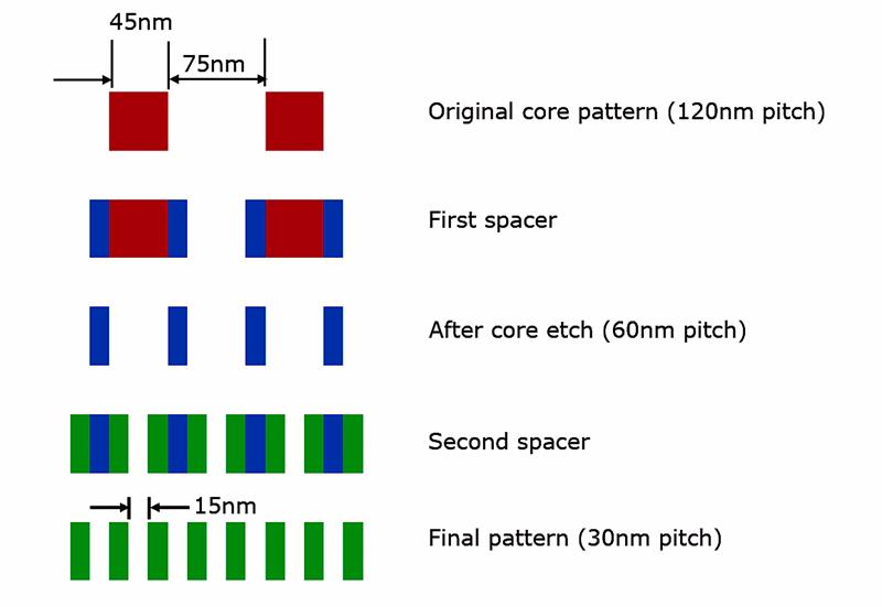
Intel has been using the idea for some time, but at the 10nm and 7nm nodes, the foundries have come round to the same idea of self-aligned multiple patterning. The latest iteration is self-aligned quadruple patterning (SAQP), a technique needed for the finely wired metal layers that sit closest to the transistors themselves.
The main technique in use is sidewall image transfer. First, relatively widely spaced lines are exposed to form a grating-like pattern in a resist material that sits on the surface of the wafer. A second resist is then grown over the top. A selective etch eats away the flat surfaces of this upper film to leave sidewalls along both sides of the first resist. A second etch removes the original lines, leaving parallel pairs. A further round of sidewall formation doubles the lines again.
No matter how finely patterned, a grating by itself is not useful for defining routes in metal. Self-aligned patterning goes hand-in-hand with so-called one-dimensional routing. To make this possible, the EDA companies have reworked their tools so they try to place logic cells in such a way that most connections are fairly simple, preferably using just one straight line. If turns are needed, wiring needs to be formed on more than one interconnect layer. Vias between those lines increase resistance and this can become so bad that some circuits need to use groups of parallel vias to make the connections, at the cost of a loss in circuit density.
There are also tight restrictions on how densely cuts can be packed before additional masks are needed. This has a knock-on effect on the freedom enjoyed by place-and-route tools. A small change to the logic can lead to cells being moved large distances, just to find a printable path.
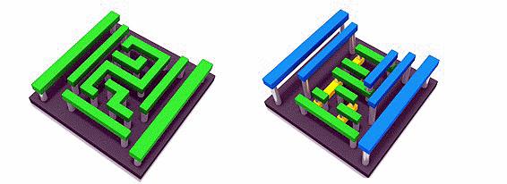 While one dimensional routing is preferable, many circuits need to use 2D routing to create a workable solution (Above)
That is not the only problem of one-dimensional routing; many routes wind up using three or more vias simply to get from A to B. At such tiny geometries, what should be a right-angled turn across two metal layers turns into two unconnected lines because the via misses one of them or even hits part of the wrong line. Once again, chemistry comes to the rescue.
Because of the way in which spacers are formed, pairs of them bend towards each other at the top. Changes to process conditions make spacers with more consistently vertical shapes, removing one of the sources of misalignment.
Another technique proposed by Intel, and supported by process-equipment vendors such as Applied Materials, is to use pairs of materials to form spacers that react differently to etch conditions. Adjacent lines are protected by materials that react to one etch process used to form the hole for the via, but not the other. Chipmakers can afford to expand the contact area used for the via to provide more scope for movement, but have a good guarantee that it will not wind up shorting an adjacent wire.
EUV potentially can make lithography for 7nm simpler. At least for now, and with a little optical proximity correction, it only requires one mask. But EUV has been so delayed that manufacturers now talk of it as being a point solution. To proceed any further, if any lithography technology can, EUV will need the same kind of double-patterning assistance as the nodes that followed 28nm. EUV has other problems that may make DUV more attractive, even in fine-geometry layers, despite the cost of using multiple masks for each critical layer.
Resists are far more sensitive to the high-energy photons of EUV than to those made for DUV. Because relatively few photons complete an exposure, the resists make patterns that exhibit more variability along their edges. Such line-edge roughness contributes to alignment problems, as well as performance.
Although the introduction of EUV would make it possible to go back to the relative freedom of two-dimensional routing, foundries are unlikely to want to force another change on customers. Instead, EUV will be used largely to reduce the number of mask steps needed for the first two or three metal layers, with DUV remaining in place for the rest. The high cost and low throughput of EUV will constrain how much fabs can make use of it.
At one point, directed self-assembly (DSA) techniques were touted as mechanisms that could push DUV further beyond 10nm if EUV failed to materialise. Sidewall image transfer is arguably a simple form of DSA. The more advanced concepts have shapes that form naturally from polymers around parts of the wafer marked out by lithography.
Potentially, DSA could form the kinds of turns and connections that SAQP patterning lacks. But the defect rates are so high as to be impractical and may only wind up in low-cost memories where it is possible to use redundancy to deal with zones that do not self-assemble properly. Even so, the kind of chemically assisted patterning of which DSA is a subset looks to be here to stay.


