
This registration comes as trends toward higher power density and cost optimisation have started to dominate high power application development, and this move will help to solidify Infineon’s goal of establishing a broad adoption of TSC in new designs with one standard package design and footprint. In addition, this move provides flexibility for OEM manufacturers looking to differentiate their products in the market and take power density to the ‘next level’.
“As a solutions provider, Infineon continues to influence the semiconductor industry through innovative packaging technologies and manufacturing processes,” said Ralf Otremba, Lead Principal Engineer for High Voltage Packaging, Infineon. “Our advanced top-side cooled packages bring significant advantages to the device and system levels to fulfil the challenging demands of cutting-edge high-power designs. Package outline standardisation will help ease one of the main design concerns of OEMs for high-voltage applications by securing pin-to-pin compatibility across vendors.”
The JEDEC organisation has, for over 50 years, been leading in the development of open standards and publications for the microelectronics industry for a broad range of technologies, including package outlines.
JEDEC has been widely accepting semiconductor packages such as the TO220 and TO247 through-hole devices (THD), devices that have been prominently used over the past decades and are still an option in new onboard charger (OBC) designs, high voltage (HV) and low voltage (LV) DC-DC converters.
The registration of QDPAK and DDPAK surface-mounted (SMD) TSC package designs signals a new era for package outlines ushering a wide market adoption of the TSC technology as a replacement for TO247 and TO220, respectively. With the benefits of this technology, this new JEDEC package family registration, according to the MO-354 standard, serves as a key enabler for the transition of high-voltage industrial and automotive applications to top-side cooled designs in next-generation platforms.
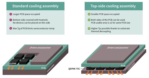
To facilitate design transition for customers from the TO220 and TO247 THD devices, Infineon has designed QDPAK and DDPAK SMD devices to deliver equivalent thermal capabilities with improved electrical performance.
Based on a standard height of 2.3 mm for QDPAK and DDPAK SMD TSC package for HV and LV devices, developers are now able to design complete applications such as OBC and DC-DC conversion with all SMD TSC devices measuring the same height. Compared to existing solutions that require a 3D cooling system, this facilitates designs and reduces system cost for cooling.
Additionally, TSC packaging offers up to 35 percent lower thermal resistance than standard bottom-side cooling (BSC). By enabling the use of both PCB sides, TSC packages offer better board space utilisation and at least two times more power density.
The thermal management of the packages is also improved by thermal decoupling from the substrate since the thermal resistance of the leads is much higher compared to the exposed package top side. Because of the improved thermal performance, stacking different boards is not necessary. Rather than combining both FR4 and IMS, a single FR4 is enough for all components and also requires fewer connectors.
These features deliver an overall bill of materials (BOM), which ultimately reduces overall system cost.
In addition to improved thermal and power capabilities, TSC technology also offers an optimised power loop design for increased reliability. This is possible by the placement of the drivers, which can be placed very close to the power switch. The low stray inductance of the driver switch loop reduces the loop parasitics and leads to less ringing on the gate, higher performance and a smaller risk of failures.


