
However, due to problems of heat dissipation, we have yet to see widespread use of combined processor and stacks. It’s a different story in the world of sensors, where amplifiers and post-processing circuitry routinely communicate with sensors on a top layer of silicon using through-silicon vias (TSVs).
The TSVs in these chip stacks do not just reduce the losses that might be incurred by sending analogue signals to external circuitry, they also make it easier to feed highly parallelised signal-processing engines that are used to improve image quality and perform functions like compression.
The front image sensor in Sony’s Xperia XZs pushed the stacking to three layers in 2017 with the addition of a DRAM under the sensor and DSP chips that is used to hold frames temporarily before being read out. The result was a sensor that can by itself support the high frame rates needed to deliver extreme slow-motion effects in movies.
Though these sensor design involve novel packaging concepts that are now spilling over into logic integration in the core computing devices in high-speed systems, the core architecture of the assisted sensor remains quite traditional: sense; digitise; process; and transfer. But what if you could move at least some of the processing in front of the digitisation step?
As an architectural approach, it is not likely to have much effect on the high-resolution imagers like the Xperia devices, but it could make it much easier for systems that rely on small batteries or energy harvesting to do a lot more with less digital processing performance. It also has a strong overlap with the idea of in-memory computing where analogue circuitry replaces more complex, power-hungry digital elements such as multipliers. As with in-memory computing, machine learning is one of the possible applications. Doing the analogue processing straight after capture avoids the need to convert data back from analogue before taking advantage of the simpler, though potentially quite noisy analogue circuitry.
One example of this kind of analogue sensor-based computing appeared earlier this year out of Harvard University’s John A Paulson School of Engineering and Applied Sciences (SEAS).
Donhee Ham, professor of electrical engineering and applied physics, and colleagues developed a silicon photodiode array that can perform simple noise cancellation or edge detection without external assistance. This works by electrostatically “doping” the photodiodes: applying bias voltages to gate electrodes above the diode terminals. This biasing affects the sensitivity of the diode to the incoming light and so alters its output. To perform filtering the voltages are altered according to a convolution kernel that can, for example, perform basic high-pass filtering to enhance edges in the resulting image or blur the input to reduce speckle noise. In the experiment, the team only had a nine-photodiode array. They employed this to build a simple 3x3 patch for the filter kernel that was, in effect, slid under the pixels of a 256x256 input image. But using this they were able to stitch together results that implemented the behaviour of conventional Gaussian blur and Sobel edge filters, among others.
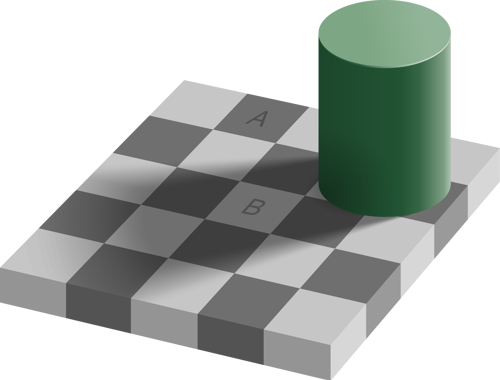
Above: Checker shadow illusion - An optical illusion by H. A. Square A is exactly the same shade as Square B
Core idea
The core idea of pulling analogue processing into the sensor dates back to an early 1990s paper by Carver Mead and Misha Mahowald working at the California Institute of Technology (CalTech), in which they took observations from neuroscience as their inspiration for building smarter image sensors. “Many of the most striking phenomena known from perceptual psychology are a direct result of the first levels of neural processing,” they wrote, pointing to some famous optical illusions as examples of how the evolution of this first layer of neurons affects our interpretation of the world seen through our eyes.
The Cornsweet illusion, one that makes it seem as though a grey area on one side of a gradient is darker than an identical patch elsewhere in the image, helps demonstrate how the human visual system perceives objects as the same despite large changes in lighting conditions. Changes in materials and sensor design could be used to deliver some of these characteristics relatively easily. Although there are good reasons for trying to stick with silicon as in the SEAS work, there are alternative materials that can be electrically tuned or adapt to inputs more easily than silicon. One way of using these material properties is to deliver superlinear response so that the sensors respond better to bright sources.
One example is molybdenum trioxide, used in an experiment by a group working at Hong Kong Polytechnic University. This reacts to high levels of light by moving to a more conductive state that increases its output when hit by more photons and which stays there for a while before returning to its basic chemical state. The result would be a sensor that suppresses low-level noise in dark areas of the image but which has a high degree of sensitivity to brighter elements.
Pain perception, in which nerves become more highly sensitised to inputs after a sudden surge, provides another biological inspiration for in-sensor computing. For this nociceptor type of response various groups have proposed using memristors on the outputs of the sensor elements. When the input stimulus is below a threshold, the memristor suppresses it but will pass on anything once that threshold has been surpassed before gradually relaxing back to the no-output state. This type of sensing would suit situations such as hazard detection where the likelihood of being triggered is quite low. One example pursued by a group in Shenzhen was to make a nociceptor that would respond to high levels of ultraviolet light and trigger an alert.
Letting the sensors interact with each other opens the door to performing machine-learning functions within the array. Though it is one of the applications that could make in-sensor computing a widespread technology, it is trickier to achieve than some of the simpler materials-based responses for several reasons. The devices need some way of modulating sensor output dynamically using external signals, though electrostatic doping of silicon similar to that used in the SEAS filter is one option, as well as more complex wiring.
Black phosphorus – a 2D material similar to graphene and molybdenum disulphide (MoS2) – may prove to be a useful material for dynamic biasing. Though black phosphorus is limited to sensing photons in the infrared range, it is possible to tune the bandgap and with that the frequencies to which it responds by controlling the thickness of the core layer. A team at the University of Washington in Seattle built a simple neural-network array using black phosphorus under layers of aluminium and hafnium oxide dielectrics that acted as gate electrodes to modulate the responsiveness of the core photoelement. One configuration performed edge detection similar to that used with the SEAS device with a more complex circuit used to process the output photocurrents that are then delivered as neural-network weights to the biasing gates.
An easier computational task might be encryption by taking advantage of natural variability in the sensor elements themselves. Physically unclonable functions (PUFs) rely on small differences in behaviour to generate unique codes for embedded systems. Instead of digitising a signal and encrypting it using a key derived from a PUF in main memory, a sensor array itself can act as an encoder for inputs. Making each PUF stable is difficult with conventional materials so some workers have used MoS2 and similar 2D materials to make more reliable photodiode-encoder combinations that may one day support self-encrypting sensors.
In-sensor computing remains a research topic but as the experience with 3D integration has shown, these front-end devices have proven to be fertile fields for innovation. The emphasis on low-energy computing could be the driver that sees more extensive analogue circuits pulled into the front-end to take advantage of novel material properties and device structures.


