
When Intel decided earlier this summer to rename its process nodes, its target was not to bring the scheme into line with the reality of Moore’s Law but to prevent the company from appearing to be further behind the curve than Samsung and TSMC than it did before. With the 20A and 18A processes meant to debut in the middle of the decade, the chip giant has brought the names a little closer to the actual on-silicon measurements though not by much.
The reason for the on-going discrepancy goes back more than two decades. Up to the mid-1990s, the name of a process node was given by the drawn length of the smallest gate on the device. At 0.35µm, the gate worked out a little shorter than that but that was the dimension. By playing with phase and other optical properties, chipmakers then found they could make the gate far shorter and benefit from speed improvements. By the time of the 0.13µm or 130nm process, the gate could wind up being less than half as long though the spacing between transistors remained as predicted by Moore’s Law.
At this point concerns over power lost through leakage caused by short channels came to the fore. By 2012, gate length scaling had stalled. It only restarted thanks to the introduction of finFETs but scaling of the gate has proceeded slowly. Chipmakers, however, have ploughed on with the traditional approach to naming.
By the end of this year, TSMC expects to be sampling chips made on a nominal 3nm process but the gate length is likely to be at least five times longer. Even the scaling of the space between devices is grinding to a halt. By the end of the decade, according to the IEEE International Roadmap for Devices and Systems, the distance between adjacent silicon-based transistors will get more or less stuck at 32nm, an improvement of just 30 per cent over today’s leading-edge processes, and gate length as well will stop at around 14nm. Despite that, Samsung and TSMC look set to name 2028’s node ”0.7nm”.
This apparent roadblock to Moore’s Law is not quite what it seems. In the past decade, the pendulum has swung dramatically away from 2D scaling towards circuit cleverness and the use of 3D structures to try to pack more into a given area. In principle, scaling can continue into the 2030s by stacking transistors on top of each other, following in the footsteps of flash memory which started this process a decade ago with a radical change to the way the transistors are formed.
The problem for logic and analogue circuitry is that they need far higher performance than the types of device that a flash memory can make. Another is that silicon transistors are not easy to stack. The amount of heat needed to repair the defects caused by doping and other processes makes it hard to avoid harming transistors formed on lower layers. By the end of the decade, chipmakers may have found an alternative.
An alternative approach
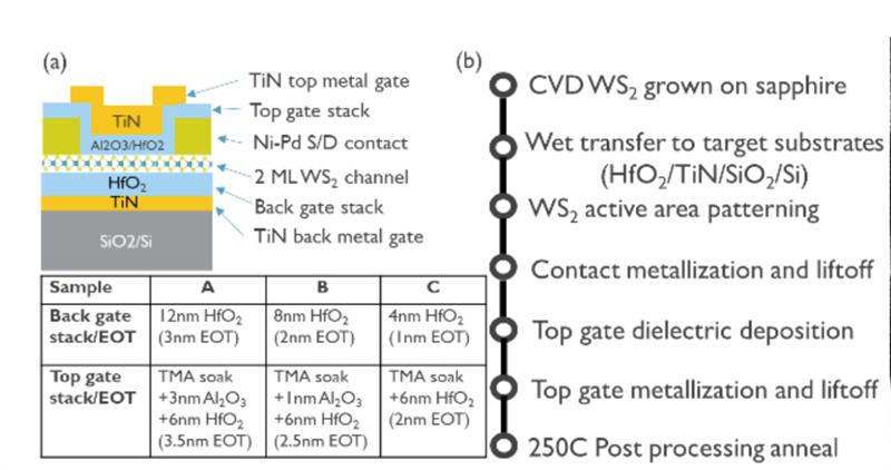
For some years, process engineering teams have focused on displacing silicon in the transistor’s channel with III-V and other materials that exhibit better mobility and so do not suffer as badly when the width and depth are scaled to nanometre dimensions as they have to be in nanosheet fins. By the 2nm generation, these nanosheets will be stacked on top of each other, pushing chipmakers to employ ultrathin structures. One option is to switch to a material that benefits from being used as a single atomic layer. One early option was graphene but it needs additional processing to work as a semiconductor and remains tough to deposit precisely on wafers.
Luckily, graphene is just one of a growing family of materials that rely on the precise arrangement of their atoms in a monolayer to exhibit useful electronic properties. The key to graphene’s impressive conductivity lies in the conical electron orbitals that form above and below the carbon nuclei in its flat lattice. These Dirac cones overlap with each other and provide an almost zero-resistance pathway for electrons to pass from one end to the other. Unfortunately, the band structure of graphene makes it impractical for use as a semiconductor: it is simply way too conductive.
One alternative that turned up a decade ago was the lubricant molybdenum disulphide. The material has a reasonably large bandgap at around 1.8eV, becoming a direct bandgap when it is used in very thin forms. It may prove easier to deposit reliably on wafers than graphene though it is not without its problems. Too much strain from the surrounding crystal surface and it starts to behave as a metal rather than a semiconductor.
In recent work, researchers at Imec have been focusing on some of the other disulphide options, principally one with tungsten on the basis it should deliver higher carrier mobility. The work so far suggests 2D materials like these could restart gate-length scaling for a few more generations before pushing the focus back onto stacking. The need to maintain some degree of compatibility with silicon nanosheets will likely lead to a great deal of attention being given to find ways to stack the thin sheets between insulating layers reliably.
Work by Imec presented at the VLSI Technology Symposium in June indicated the processes would survive temperatures up to 400°C, which would let chipmakers form the transistors in the metal layers and not have to restrict them to the wafer surface.
One big problem though for these 2D materials is getting electrons in and out: contact resistance remains a major roadblock. The sulphur atoms tend to form unwanted chemical bonds with the kinds of metal often used in contacts, such as tungsten, changing the bandgap. One option might be to try to apply graphene to contacts that land on top of the material at either end of the transistor, though this brings back the production problems that manufacturers have already identified.
Even so, graphene may well wind up being used in other parts of the chip: the transistor is not the only problem for post-1nm processes. Interconnect resistance continues to rise simply because the printed wires are becoming too thin to support the current flows required. Conventional metals are running out of steam because the boundaries between crystal grains dominate the total resistance even if the bulk conductivity is good. Graphene may turn out to be the best choice for the densest interconnect layers.
At IEDM late last year, a team at the University of California at Santa Barbara described how they found a way to make multi-level graphene interconnects on top of a silicon dioxide and copper substrate, a potentially important step because it is broadly compatible with existing techniques for making on-chip interconnects.
Other forms of topological 2D material could substitute for graphene here as well. Topological semimetals have unusual band structures that favour electron movement through specific paths through their crystals, similar to the surface transport of graphene.
When you take the grain-scattering effects seen in metals into account, semimetals start to look a lot more promising. In a paper at IEDM, IBM researchers indicated alloys such as niobium arsenide or cobalt silicide could cut line resistance by as much as half compared to copper and tend to show advantages as line thicknesses scale down.
The downside is, once again, manufacturability. No-one is yet sure how compatible these unusual materials will be with the processes used to form interconnects though they and close relative topological insulators have novel magnetic properties that would support a transition away from charge-based to spintronic transistors.
Though there are plenty of materials problems to solve, the increasing use of vertical stacking to push silicon CMOS as far as possible gives process engineers close to a decade to find a way forward.
If successful, the 2D options will help 2D scaling move forward by one or two generations but more importantly provide the basis for far more extensive 3D integration.


