
Silicon scaling remains alive and well, just as long as you can pay the increasing healthcare bill that keeps it that way. Area scaling inevitably has to stop. For some aspects of transistor design and routing, that is fast becoming the case.
According to the current edition of the IEEE International Roadmap for Devices and Systems, reductions in transistor gate length will stall in the second half of this decade. There is some room to manoeuvre for spacing between transistors. But that inevitably is flattening out. The local routing used within standard cells will not shrink further once the successor to the 2nm node is in place sometime around 2028.
How then to do more in less space? The key is to turn to a series of tactical nips and tucks that improve density without changing the core dimensions much. One big target is the power infrastructure that every transistor needs to operate. This grid of power and ground rails brings with it a large area overhead, not least because the metal traces employed have to be fatter than signal lines to avoid incurring too much resistance.
Imec proposed burying these rails several years ago, as a prelude to doing something that power-transistor manufacturers have done for many years: use the backside of the wafer to lay down a metal grid that can deliver high power at low resistance. In its own experiments on moving the power grid out of the way of the topside metal layers so they can be dedicated to logic signals, Samsung Electronics found it could cut area by up to 19 percent in work the company’s engineers presented at VLSI Symposium in the summer.
The transition is far from straightforward, though. To avoid high-resistance vias from the back of the chip to the topside transistor, the wafer needs to be thinned down to less than a micrometre. Even with that reduction in wafer depth, embedding the vias for power has its issues. And chipmakers are trying out various ways of dealing with them.
New techniques
The first technique to make it to market is a halfway house to backside power delivery: the buried power rail used by the Intel 4 process. This carries power using metal conductors placed in trenches etched into the wafer, but the supply rails come from the top side of the chip.
Because these rails are formed early in the manufacturing process, it is relatively straightforward to align the transistor source and drain contacts on top. That is not the case for the backside-power options, which face more difficulty in placing the contacts. This is a major factor in why buried power rails are coming first. But resistance trade-offs play a large role in density and performance.
Copper would be a better metal for the buried rails, but it would not survive the 1000°C process steps needed to form working transistors on top. Instead, the best options seem to be tungsten, already widely used in the vias that carry power and signals from the metal grid to the transistors, or ruthenium, which is expensive and less proven in manufacturing. Making the buried rails comparatively tall, perhaps with an aspect ratio as high as seven, will help. But the resistance within the buried rails and the lower metal lines that take power down to the chip surface mean tap points, which are quite large, will have to be placed roughly every 10 or 20 transistors or so apart. That will eat into the area budget.
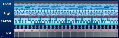
Above: A schematic cross-section of imec’s back side-power/processor/memory stack
The second option is a “via middle” scheme for backside power delivery. Here, the power is taken through a long, through-silicon via (TSV) connection from the back of the wafer to a tap point in the topside metal grid. This is the approach showed by Intel at VLSI Symposium on wafers put through a modified Intel 4 process. Calling it PowerVia, Intel uses two wafers bonded together so that it can make the top and bottom metal grids separately and then join them once the top wafer has been thinned, which avoids many of the problems of high temperatures.
The third approach is to deliver the power to the underside of the transistor directly instead of taking up precious space with vias and connections to the topside metal grid.
This last approach is the toughest to achieve. The contact size of a direct contact to a transistor source or drain is significantly smaller than the topside metal lines used today for power routing. At this level of precision, warping on either of the bonded wafers presents a major issue, with a high risk of shorts if vias miss their contacts.
Despite the obstacles, Imec expects that underside delivery may be the only realistic choice to deliver further area savings from backside power routing once chipmakers have reached what Imec calls the A14 node. This is the node the research institute expects to follow the N2 or 2nm generation. The expected scaling in cell track height will probably leave insufficient space for per-cell TSVs.
Complementary field-effect transistors
While the power goes in from the bottom, transistors are set to move up in the stack with the complementary field-effect transistor (CFET), another concept proposed by Imec several years ago.
This is an approach that has issues with manufacturability. But it is one of the few that can keep scaling on track by almost doubling density with that one major change. The big issue is that the high annealing temperatures needed to repair the damage caused by successive deposition steps and create a working upper transistor will degrade the finished transistor underneath.
In the description at the International Electron Design Meeting (IEDM) this month of a design that places an n-channel transistor over a p-channel counterpart, TSMC engineers showed the transistors had a 90 percent survival rate, which is progress but some way from production viability. In its presentation, Intel coupled a similar layout with backside power delivery using direct backside contacts.
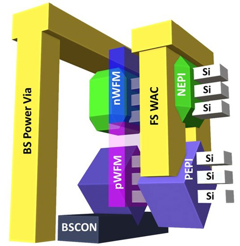
Above: Intel’s CFET-backside-power combo
One issue with the CFET is that having paired n- and p-channel devices matched in size reduces the freedom that designers have to construct logic and analogue circuitry. That situation is not helped by the differences in mobility and, therefore, performance between the two types of transistor.
Intel has an answer for this at the manufacturing level. The process described at IEDM makes it possible to remove the semi-conducting nanosheet channels inside each transistor selectively, disabling one or the other and allowing the size to be optimised for the remaining device, at the cost of some density. Designers may find they can avoid the need to add this complexity to fabrication.
Work by a team at Fudan University, China found choosing between two ways of wiring together the paired devices can support a usable set of standard cells and SRAM bits.
A further spinoff benefit of the vertical approach to power and logic may come with memory integration.
According to Imec, the use of backside power delivery using TSVs makes it easier to build the kinds of logic and memory stacks needed for AI and high-performance computing. A relatively small number of TSVs can go all the way through the logic chip into a memory chip placed on top.
In this architecture, the memory and logic wafers would be bonded face-to-face and the logic wafer joined to the power-delivery carrier chip. Overheating may prove to be an issue: thinned silicon does not distribute heat well and the most active chip will be further from any heatsink. But the reduction of logic and memory distances made possible by 3D may prove to be a better trade-off in both performance and power consumption.
Given the roadblock that faces 2D scaling itself, chipmakers may not have much of a choice in the matter.


