Together with colleagues from MIT, TSMC, UC Berkeley and his own institution, Philip Wong, professor of electrical engineering at Stanford University, wrote a paper for April's Proceedings of the IEEE on the progress made by silicon scaling and used it as the basis for his keynote at July's Design Automation Conference. In their view, Moore’s Law is still in operation but the assumptions that underpin it have changed. As a result, technologists should look far less at simple areal scaling of transistor footprints and spacing but take a view on the effective density of each successive node.
In looking at other factors, you could argue that the chipmaking industry is going back to basics. It is less famous than the article in Electronics magazine published a decade earlier, but Gordon Moore’s speech at the 1975 International Electron Device Meeting (IEDM) is the point at which the Intel executive settled on a two-year cadence for the regular doubling in device density. Up to that point, the industry had been moving at a faster clip, with doubling occurring on an annual basis. By 1975, Moore had seen that the rate of progress was dropping.
In the IEDM speech 45 years ago, Moore saw 2D geometric scaling as only part of what would deliver double the functions for the same cost over time. He saw it as a sizeable fraction but certainly not all of it. He predicted significant increases in chip size and improvements in circuit design would deliver the rest. However, at that point, the fab owners had only begun to take advantage of scaling factors noticed by IBM researcher Robert Dennard: that smaller, more closely packed transistors would be able to not just achieve cost but energy improvements.
The transition to CMOS in the 1980s pushed that along at full speed until the industry had exhausted most of the benefits of Dennard scaling by the mid-2000s. After that, simple 2D scaling would become increasingly troublesome.
This has been most noticeable in recent years in the trends for SRAM scaling, which has historically been a good guide to density improvements. Though it kept pace with logic up to around the 28nm generation, it then began to fall behind because it is hard to make incremental improvements when metal pitches and transistor dimensions are not doing the same.
Circuit cleverness
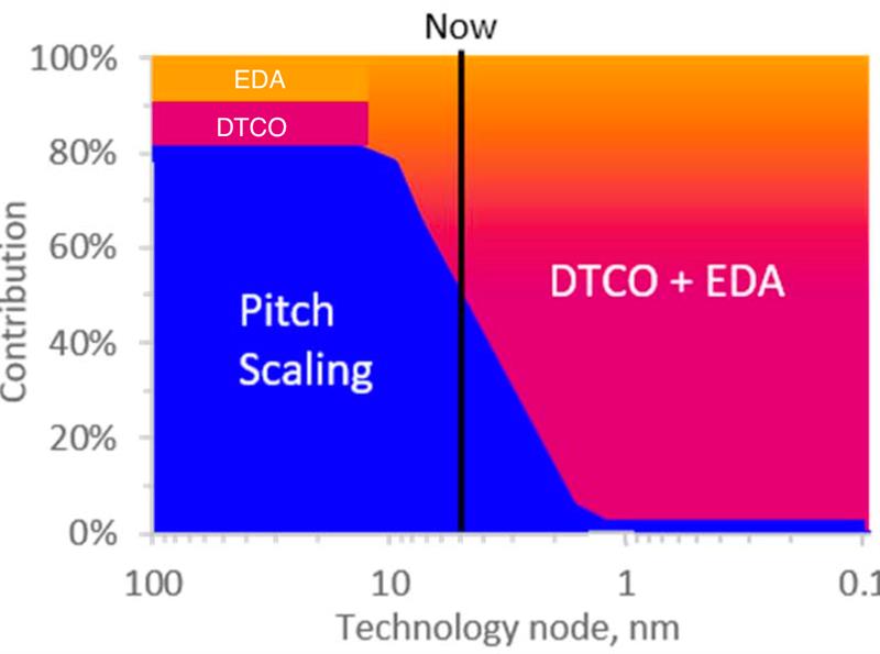
One of the presentations that takes place at the upcoming IEDM will be given by a team from EDA tools supplier Synopsys. It will show how the contributions to scaling are changing the past few years.
”Circuit cleverness” as Moore termed it has made a dramatic comeback, though in a different guise to the form proposed originally. This time around, it goes under the name of design-technology co-optimisation (DTCO). By having designers advise on what process changes make most sense for circuit layout purposes, process engineers can make better trade-offs. This is something that shows up in the SRAM scaling changes, with the odd sudden jump in density thanks to a change in the way the cells are laid out.
It is DTCO that Wong, the Synopsys team and others see as the most important contributor to density in the coming decade on the way to the so-called 1nm node. But pure dimensional scaling is not quite dead yet. Though there is little room for 2D scaling, the third dimension is showing promise and not necessarily through the stacking of chips as seen in memory standards such as HBM. You could regard it as 3D by stealth.
One way of using the vertical dimension is to turn the transistor on its side. This continues the evolution of the field-effect transistor from a purely planar device with a top gate contact through the vertical fins of the finFET. The fin provided greater electrostatic control over the transistor channel by having the gate wrap around three sides. But past 5nm, a gate all-around structure is needed. That can be satisfied by the use of nanosheets that, in effect, are passed through the gate electrode. Even better, though it increases process complexity and cost, you can stack nanosheets to get more drive current in the same way finFETs generally use two or more fins. The stack consumes potentially less area than the multifin structure.
The evolution of key vehicles of transistor density scaling in semiconductor industry extended beyond 1nm
A stumbling block to nanosheet scaling is the separation needed between the n- and p-channel devices of a CMOS pair. But Imec last year proposed the forksheet. This stacks complementary n- and p-doped sheets next to each other, built out of a common pillar. With that you have a full CMOS inverter built into single transistor structure for an area saving of about 30 per cent.
Getting power in and out of a logic cell takes up valuable area but that is another place where the third dimension comes to the rescue. Imec's proposal at the 2018 VLSI Symposia was to bury power rails under the silicon surface. The next step was the CFET: a two-storey structure that forms the n-channel transistor of an inverter directly on top of its p-channel sibling.
At the upcoming IEDM, Intel's engineers will describe their take on a CFET-type structure based on nanosheets. The combination transistor uses epitaxy to build a vertically stacked source-drain structure with the threshold voltage tuned individually for the two types of transistor. Though the gates in this work are comparatively long at around 30nm, the Intel team expects significant cell-size reductions being possible through the self-aligned stacking.
According to Synopsys' calculations, CFET does a lot for SRAM though it does take some DTCO to get there. One drawback of the CFET is that the stacking introduces another form of variability but, again, design tweaks will help deal with that. For example, the most compact structure does not rely entirely on gate-all-around transistors. Instead, it includes a dummy p-channel transistor with a three-sided gate to get a good enough write behaviour.
Major issue
Even as transistor density scales, a major issue with chip design lies in the parasitic resistance and capacitance in long metal interconnects. This may force future processes away from the mainstay of copper to more exotic metals such as ruthenium.
Intel proposes a design-based alternative that relies on the observation that although cutting resistance and capacitance together seem desirable, not all circuit paths will benefit in the same way.
Individual paths can benefit from individually tuned resistance and capacitance. This is the intuition that guided work at Intel on what calls staggered interconnect.
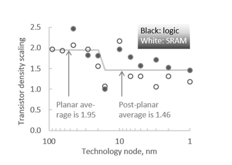
Scaling figures for SRAM and logic
Rather than make every parallel line the same, the staggered approach has alternating tall and short lines, with the short lines sitting on top of taller piles of insulator material. This reduces the net effective capacitance between lines. In effect the tall lines, which will suffer more from crosstalk and similar effects are spaced further apart. Simulations by Intel showed register files and memory arrays can benefit from the structure. Decoder and wordline memories receive the taller lines while bitlines use the shorter traces. Longer-length interconnects also show an improvement by making it possible to pack more traces into a smaller area without worsening RC delays.
The greater complexity of these DTCO-inspired designs, Synopsys says, will drive wafer costs higher: averaging 13 per cent per node. But effective density remains plausible as far as the 1nm node and it will still be possible to maintain a per-transistor cost reduction of 32 per cent per node.
It's not yesterday's Moore's Law but scaling should continue for more or less a decade. How many companies will be able to command the huge volumes to justify the start-up costs remain another matter.


