
Although a common reason for keeping passive components off-chip is their size relative to that of the transistors on-die – is not worth wasting precious silicon area on devices that cost more to assemble than their materials are worth – many off-the-shelf parts rely on passives to tune filters and control loops for specific applications.
Few designs have sufficient volume and sensitivity to circuit size to warrant the shift to integrated passives. It often make sense to trade the PCB space and circuit tolerances against setup costs. As a result, it is no surprise that the market size for integrated passives is dwarfed by that of discretes. Even though they are making inroads, the relative growth of integrated passives is only slightly faster than that of the main market.
Research & Markets expects the integrated-passives sector to grow around 8 per cent per year over the next five years. Estimates of the total passives market point to overall growth of around 7 per cent over a similar period.
Integrated passives are mostly making inroads in specific areas. Kemet sees an opportunity for its Konnekt product line in power applications. In contrast to the wafer-based production of a typical EMI filter, the Konnekt design packs together several ceramic capacitors into a stack using a liquid-phase sintering process.
The parallel array of capacitors leads to lower parasitics, with further reductions in losses made possible by placing the electrodes in parallel on the PCB, which gives the package a slightly larger footprint. The standard orientation is taller to allow closer packing.
The biggest market for integrated passives historically, commanding 60 per cent of the total in 2017 according to Yole Developpement, is for devices that filter I/O lines for EMI and electrostatic discharge.
The advantage of an integrated device is that the module can combine Zener diodes and similar active devices with passive elements to create readymade filters. As the EMI and discharge needs of parallel I/O buses tend to be similar across a wide range of applications, it is an area that readily supports standard integrated products.
Many of them use the same kind of thin-film processes as those used to form semiconductors and can incorporate active devices. As a result, traditional silicon vendors such as On Semiconductor and STMicroelectronics have a strong showing.
Extending operating range
Although ease of assembly is one motivation for using integrated passives, the use of semiconductor-type processes can extend the operating range of the circuit elements themselves. Thanks to the DRAM market’s drive for integration, etching and material-fill techniques on silicon support capacitance areal densities of more than 200nF per square millimetre.
Acquired by Murata in 2016, France-based IPDiA commercialised a process that took the traditional trench capacitor and repackaged it in a form suitable for use in dedicated integrated passive devices.
One area where the Murata devices fit is in high-temperature applications. Conventional ceramic dielectrics tend to degrade when operated over 150°C, although the liquid-phase sintered materials employed by Kemet can tolerate higher temperatures because they remove the need to use lead-based solders in the packaged part.
Silicon-based materials can survive temperatures as high as 250°C with the added advantage of supporting miniaturised form factors, suiting them to use in down-hole sensors for drilling rigs as well as in automotive-engine manifolds.
The devices have found applications in medical implants because silicon does not degrade in the body and the technology’s support for miniaturisation. Another target for the devices is in broadband optical communications because they can support frequencies that stretch into the 100GHz range.
Lower breakdown voltage is a potential issue for silicon-based devices compared to conventional capacitors when very fine structures are used. At the high end of the capacitance density range, the breakdown voltage for the Murata silicon capacitors is around 10V. But by reducing the density to less than 10nF per square millimetre, the breakdown voltage can be pushed above 150V.
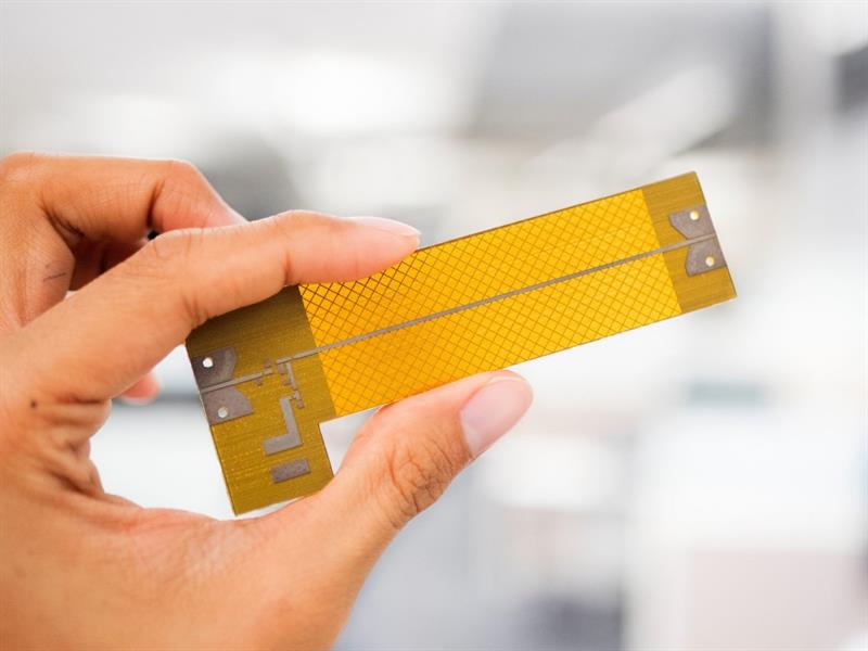
Above and top: Nano Dimension has demonstrated PCBs that incorporate printed capacitors
Although the focus has been on high-performance capacitors, Murata is looking to extend the integration to support onchip inductors and resistors to support a wider range of circuits, such as the front-end filters in mobile handsets, joining suppliers such as On and ST and a number of other recent entrants as supply chains change.
Growing competition
Packaging and semiconductor suppliers are now competing with each other rather than one simply buying from the other. ASE and StatsChippac are two packaging houses that have moved into this area by supplying foundry services to OEMs and other chipmakers. The traditional customer for front-end filters has been the handset OEM but this is beginning to change through the efforts of fabless specialists like China-based Xpeedic who are designing integrated passives built at foundries for the manufacturers of power amplifier modules.
A similar market is opening up in processors because of the need to pull power and decoupling devices into the package, another area that Murata is beginning to target with its silicon capacitors. Such passive circuitry could go into the outer organic package or through production at silicon foundries into the silicon interposers used for some advanced system-in-package designs.
Although mobile handsets are seeing passive circuitry sucked into IC packages, the need to customise systems designs means many of these parts still need to be placed on the PCB. However, space pressures can lead to the components being placing either inside the PCB substrate itself or moved to the outer package.
Over the past couple of decades, some PCB fabricators have offered technologies that encapsulate standard components within the layers of the substrate to try to free up space on the outer surfaces. An alternative is to move to in-mould electronics.
TactoTek has developed an injection-moulding process that can support surface-mount components and printed interconnects: the components are placed before the package is moulded into shape. Though heat is an issue in the thermoforming process, the company says a number of chip-scale and leadless package forms are compatible with it.
An alternative to placing components before forming comes through the advent of 3D-printing technology: create the components as part of PCB or enclosure fabrication process itself. Last autumn, following on from work to build printed planar coil inductors, 3D-printing specialist Nano Dimension demonstrated PCBs that incorporated printed capacitors ranging in storage values from 0.1nF to 3.2nF. The capacitors were printed using the company’s combination of silver conductive ink deposited alongside a polymer dielectric.
The relatively flat capacitors cover a larger surface area than conventional surface-mount ceramic parts: additive processes have a long way to go before they can make the ability to create the fine nanostructures that support the high capacitance densities of semiconductor etch-and-fill processes. But 3D printed opens up the possibilities of creating circuits on curved and irregular surfaces such as the inside of a casing that may give the manufacturer more space to play with. The printed technology has also found applications in medical devices, where they are deposited on the end of a flexible probe.
To try to carve out other niches, manufacturers of integrated passives are looking at alternative substrates such as gallium arsenide and glass to take advantage of their specific electrical and thermal properties. Though it remains a smaller corner of the overall passive market, it is gradually extending tendrils further into the core of electronics design.


