
For more than half a century, high-purity silicon has dominated the world of IC production. It’s a material that has almost everything.
Silicon is not just an effective semiconductor, it is mechanically strong. That is in direct contrast to many of the III-V materials that offer high performance but are much more fragile.
Sapphire provides strength and excellent electrical isolation, but is difficult to integrate into manufacturing economically. As a result, materials such as gallium nitride that are useful in high-brightness LEDs and power devices, have shifted from sapphire to silicon wafers.
A challenger is emerging but even that is based on silicon. Tweaks to the chemistry and manufacturing processes are now making glass a powerful contender.
One advantage that glass has is that it works well as a companion to silicon, making it possible to tune manufacturing processes and experiment with novel ways to eat into adjacent markets.
According to the market analyst firm, Yole Développement, the biggest use of glass as a substrate is in microfluidics and it is likely to stay that way into the early 2020s even as other uses develop for the material.
Although polymers such as polymethyl methacrylate (PMMA) have become popular for lab-on-a-chip devices, because they can be cheaper to process, many applications cannot use them because solvents and reagents are more likely to attack them. Glass and pure silicon are far less likely to react.
Glass carriers
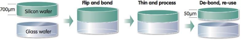
The other major use of glass today is largely hidden away. Ever since ICs were incorporated into smartcards, fabs have had to find ways to keep silicon wafers stable and flat while they etch away at the underside and then attach interconnect to the top. As it is thinned down to just a thickness of 100µm, silicon easily bends and sags. The answer is to temporarily bond the thinned wafer to a glass carrier.
One big advantage of using glass as a carrier and substrate is that subtle changes to chemical composition make it possible to match the thermal coefficient of expansion (CTE) to whatever it needs to be bonded. This, in turn, is likely to see glass move from the fab into the IC packages themselves.
At the start of the decade, Georgia Tech’s Packaging Research Center started to look at using glass inside the 2.5D and 3D multichip modules that had begun to appear in high-density smartphones, high-end networking equipment and computers.
For 2.5D and 3D packages, manufacturers were faced with two distinct choices. The first, was to adapt the existing organic-polymer materials used for low-cost IC packages to work as mini-PCBs that interconnect the multiple chips inside the module. The organic materials, however, have two problems. Although they are cheap to use, there are limits on how dense the interconnect can be. Organic packages tend to suffer from warping and stretching when heated and cooled, which can cause very thin connections to bend and then break completely. As a result, there are limits on how thin and how closely spaced interconnect traces can be, which makes it difficult to design modules that need very wide buses between devices inside the package.
The other option pursued by chipmakers up till now at a commercial level is to use silicon as an interposer. Foundries such as TSMC have redeployed older fab lines, typically those capable of producing 90nm or 65nm-generation ICs, to make interposers with an interconnect density that rivals that found on the chips themselves, albeit at higher cost. The interposers are generally entirely passive although there is potential to put switches and other active devices onto the substrate.
Georgia Tech’s PRC proposed glass as a third option that can rival the interconnect density of silicon and greater CTE compatibility but with a cost structure closer to that of organic packages. Unlike silicon, the glass does not have to be made in wafer form. Experience with LCD manufacture has led to a mature market for equipment that handles large rectangular panels. This allows more devices to be handled at a time and without the waste of cutting square devices out of a circular blank. Glass suppliers have demonstrated the ability to form substrates that measure 1m on a side, although 500mm looks likely to become a common size for packaging work.
A further advantage of glass is that it remains mechanically strong even when thinned in the same way as silicon. Even roll-to-roll processing is possible thanks to the way glass becomes much more flexible when thinned to extreme levels. The researchers have worked on interposers that are as thin as 50µm to support low-profile packages.
| Below: A schematic of the typical wafer-bonding and transfer process for silicon wafer thinning |
Brittleness a problem
But they found it was not all good news for glass. The legendary brittleness of glass and its low thermal conductivity could prove problematic. Chips are often designed with the notion that a large proportion of the heat they produce will escape into the PCB. Designers would have to rethink this if their devices were flip-chip bonded onto a glass substrate.
A technology devised to increase interconnect density in 3D packages may yet help glass become the interposer of choice by helping to deal with its problems. Through-silicon vias (TSVs) have made it possible to build dense stacks of DRAM that deliver much higher throughput than conventional memory modules. The process involves drilling or etching holes in the substrate and filling the cavity with copper or a similar conductor to connect traces from the top to the bottom surface of each device in the stack.
Through vias on organic laminates cannot be spaced much closer together than 200µm. TSVs can be spaced as close together as 10µm, though most designs will use a more relaxed pitch because the relatively thick copper traces can easily eat into space on the die that needs to be used for active logic. Work by the PRC as well as suppliers such as Corning has produced test devices on glass with through via spaced 30µm apart.
The copper conductors could help with both the problems of fragility and thermal conductivity. The metal vias will help convey heat more efficiently to the PCB. R&D teams have proposed using additional copper structures. In dense stacks, the copper could convey heat to spreaders around the edges of the package. Corning also found the thinned glass is less likely to break in areas that contain vias.
Wireless applications
Although high density could see glass begin to displace organic and silicon interposers in computing-oriented products, other properties of glass point to the early applications being in wireless communications. Glass is already used for making passive RF filters and similar devices, and has advantages in RF interconnect. The Industrial Technology Research Institute (ITRI) in Taiwan has tested interconnects useful for RF work at up to 20GHz. The group found lower losses in glass-based waveguides and microstrip lines compared to silicon substrates.
Its high resistivity favours the use of glass as a medium for carrying integrated passives that operate at the frequencies needed for 5G and millimetre-wave radio.
STMicroelectronics set up lines to make integrated passives on glass several years ago. Work by Corning and Qualcomm has looked at building high-Q inductors on glass using metal-insulator-metal architectures. The ability to pack many passives together underneath an SoC may also help see glass adopted for high-density IoT controllers.
The encroachment of glass into mainstream production has been slow up till now and almost invisible. But the push to deliver higher throughput more cheaply may see the material become a much bigger player in the coming decade.


