
The importance of integrated passives only becomes apparent when they are included in system in package applications.
An integrated passives technology initiative (iPassives) was begun at ADI, with the aim of delivering passive components that could encompass more of the signal chain while overcoming the limitations and complexities of the existing approaches used with passive components.
iPassives can be viewed as a flexible design tool that enables the design of system solutions.
Integrated passives technology is being used to tie this all together in highly customisable networks and packaged up via system in package technology to create µModule devices.
Passives generally constitute over 80% of the bill of materials in an application, occupy about 60% of the area, and make up about 20% of the overall component spend.
There is often a high degree of uniqueness to components and that can contribute to errors that degrade time zero circuit performance across the operating lifetime of the circuit. The assembly and wiring of individual components also takes time.
The elements are connected using a soldering process, generally through-hole or surface-mount technology (SMT) assembly that has enabled the development of smaller passive components; in this case, a landing pattern is etched on a PCB, solder paste is used to cover the patterns, and then SMT components are positioned using a machine.
The PCB is then run through a soldering reflow process, where the solder liquefies and establishes electrical connections, and, when cooled, the solder solidifies and mechanically affixes the SMT components to the PCB. The primary problem is that soldering processes can be very unreliable.
The actual composition of the solder, mechanical stability during the solder reflow process, the purity of the solder and the time and temperature in the solder reflow process can all have an impact on quality.
Another limitation in employing passive components is that trace lengths need to be long, which can introduce unaccounted for parasitic elements that can limit performance and the repeatability of results.
Passive devices also present a lot of potential contact points where ESD events can occur.
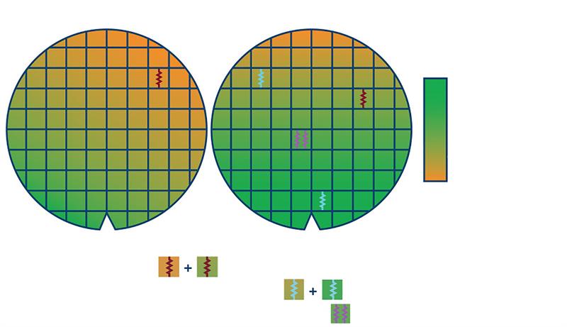
Figure 1: Matching of discrete vs. passive resistors. |
Integrated Passives
Integrated circuits contain many transistors wired together with very well defined metal interconnections. Special processes have been developed for analogue type applications like DACs and ADCs that contain portfolios of passive components in addition to the transistors. To achieve the performances required, very high quality passive components have been developed and these are used to build integrated passives.
Just as integrated circuits contain many transistors, integrated passives can contain many high quality passive components packed into a very small area. They are fabricated on large area substrates where multiple passive networks are produced at the same time.
One of the most compelling advantages of integrated passives over discrete passives is the precise matching that can be achieved with them. When integrated passive networks are fabricated, all components within a network are manufactured at the same time, under the same conditions, with the same material set and, because of network compactness, essentially in the same place.
To illustrate this let’s say we have an application that requires two matched resistors. These resistors are fabricated on circular substrates such as silicon wafers (Figure 1).
Due to slight process variations like resistive film thickness, chemical properties of the film, contact resistance, etc., there will be some level of resistance variation within a batch and even more variation across multiple batches. In Figure 1, dark green indicates the resistance is on the high side of the tolerance range and yellow indicates the resistance is on the low side of the tolerance range. For standard discrete devices, there is the possibility that each of the two resistors may come from different fabrication batches as indicated by the two separate resistors drawn in red. The full tolerance range of the process may be observable between the two discrete resistors and hence the matching will not be very good. With special ordering restrictions it may be possible to have the two discrete resistors chosen from the same batch as indicated by the two separate resistors drawn in blue. The tolerance range within just one batch may be observable between the two resistors. While the matching between these resistors will be better than the random discrete case, there is still scope for some level of mismatch.
Finally, with integrated passives, the two resistors come from the same die, as indicated by the resistors drawn in black in Figure 1. The tolerance range within one die is the only range that will be observable between the two resistors. Hence, matching between the two resistors will be excellent.
The individual components within integrated passives are placed closely together and, because of this, the interconnect parasitics such as trace resistance and inductance can be kept to an absolute minimum.
On PCBs, interconnect parasitics can be variable due to trace tolerances and component placement tolerances. With integrated passives, interconnect tolerances and component placement tolerances are extremely tight due to the photolithographic processes employed in their manufacture.
The miniaturisation of passive networks through integrated passives has the added benefit of making circuit boards smaller, reducing circuit board costs and allowing more functionality and performance to be added. Building systems with high channel counts becomes much more practical when using integrated passives.
Another significant advantage of integrated passives is the robustness of the complete wiring network around them. Rather than needing lots of soldered connections, integrated passives are essentially forged together in one complete unit, sealed up with glass, and then further protected with a robust plastic encapsulant.
An additional benefit of integrated passive networks being so well sealed up is that the number of exposed nodes in a system is much reduced.
Integrated passives, having multiple passive components within one device, greatly unburdens the customers’ bill of materials, which results in the cost of ownership going down. Customers receive integrated passive networks fully tested and proven to be good.
High quality passive devices have been core to the circuit performances achieved by many of ADI’s products and the integrated passives portfolio now contains a significant number of components.
The integrated passives process is modular, which means that the processing steps needed to produce a certain type of passive device need only be performed if that particular component is needed. An iPassives network can essentially be built up with just the processing complexity required. There are a number of passive building blocks to choose from and constructing an integrated passives network can be as simple as piecing together the required components.
Integrated passives hold many advantages over discrete passives and ADI’s µModule devices leverage off the capabilities of a diverse range of integrated circuits.
These circuits are manufactured through tailored processes that provide enhanced performance and that are not achievable from any one single process. ADI is using iPassives to tie these integrated circuits together and in doing so are building complete precision signal chains within a single device.
By adopting a reusability approach from a huge portfolio of field proven ICs and combining this approach with the versatility of iPassives, both the development cycle times and costs are dropping significantly.
At first glance, the use of integrated passives may appear only incrementally more advantageous over established approaches but, in truth, they turn out to be significant and iPassives are redefining what can be done, but also what speeds, costs, and sizes are beneficial to customers.
Author details Mark Murphy is a product marketing engineer with Analog Devices’ Precision Converter Group, while Pat McGuinness is a product engineer at Analog Devices with responsibility for the use of integrated passive components. |


