
As there is more integration of functionality onto silicon, more resistors and capacitors for signal and power integrity are required, leading to even greater board congestion.
So what constitutes good PCB design?
"That depends entirely on the perspective of those involved. Classically, the PCB designer, or 'lay-outer', and the management team will take up opposing positions," suggests David Wiens, business development manager, Mentor Graphics. "Traditionally, PCB designers tend to focus more on the 'artwork' than either its manufacturability or performance. By contrast, management will focus on whether the design functions as expected, the costs and how quickly it goes into production. Their focus is solely on performance."
The biggest challenge for PCB designers today is they now have to consider multiple and variable performance issues: signal or power signal integrity; manufacturability; and overall cost.
"All of these issues can conflict and will constrain the designer. Today, they have to accept that design trade-offs exist and have to be addressed. It also requires driving more validation into the design process and that means more virtual – rather than physical – prototyping to assess options," Wiens suggests.
One thing is certain: PCB designs will not be getting simpler any time soon.
"As designs become more complex, so those doing the layout have to change," believes Wiens. "That is not to say that classic layout designers are not equipped to deal with the challenge, but they certainly need to be capable of 'stepping up to the plate' and having the right skills to assess the different variables that will need to be considered in terms of modern board design."
Power and thermal management are critical, says Wien, with both being driven by developments in silicon.
"To get lower power out of ICs, designers are creating and using more differentiated voltage rails. In PCBs of 10 to 15 years ago, ICs may have had four voltage rails at most. Designers would look to short them together on the PCB, so running only one or two voltage rails on what was essentially a clean PCB layer. That design could support a current return and a clear path for efficient power distribution.
"Today, you have to work with designs with up to 50 voltage rails on the silicon which means something like 25 voltage rails on the PCB. BGAs on the top layer can lead, in turn, to what we call the creation of a 'Swiss cheese' effect – fanning out that leads to fragmenting of the PCB and the ability to distribute power is compromised as a result. It's a big issue."
|
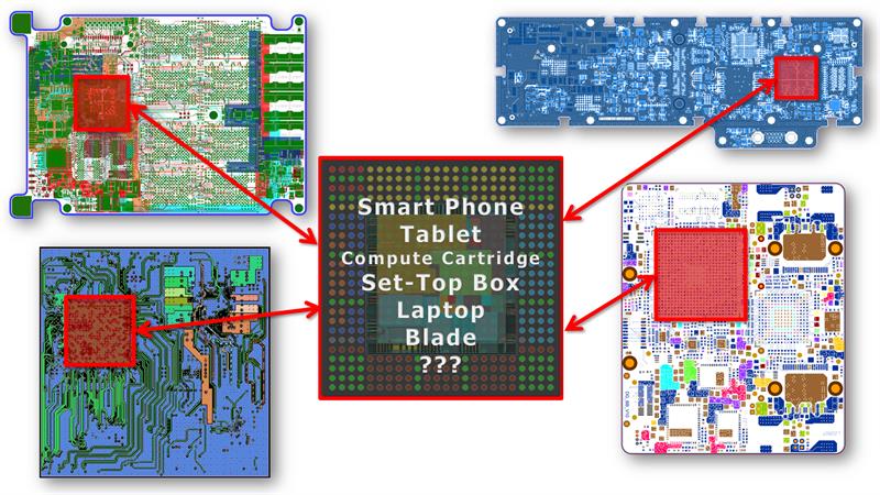 Multiple target platforms (PCB form factors) can be considered during chip/package planning and optimisation
Best practice does exist, but will depend on the voltages in use, the tolerances required and the board's geometry.
"Eight years ago, no one conducted power analysis of PCB boards. Today,more than 85% of designs not only address power integrity, but also signal integrity and manufacturability," Wiens says. "And the easiest way of addressing this is through analysis."
Going forward, PCB designers will look to not only push tolerances, but also the geometries being employed.
"In the past, different configurations were employed on different boards; today, most layouts look the same. Designers are mixing power with signal distribution – board layout is intertwined. From a manufacturing perspective, that's not a problem. You're taking a piece of copper and simply hacking it up for signal and power.
"The big issue with modern PCB design is thermal management," Wiens contends.
"Designs employ multiple rails operating at higher currents, so they are getting hotter and hotter. You have to look at the board and consider what techniques should be employed to better conduct that heat. You need to consider 'shadowing'; how chips sitting next to one another on the board impact each other. Thermal conditions will play a crucial role in terms of the design's impact in both power and signal integrity."
According to Wiens, simulation provides the opportunity to better consider all these issues.
"It's vital that you think about all these things at the same time and not in isolation.
"It is what has been described as the 'continuous push left', it's about driving the decision making process further into the design stage before you actually have a physical design," Wiens explains.
In terms of the design process, virtual prototyping will enable earlier validation and support improved trade-off analysis making the process more efficient.
As board layout becomes more complex, so partitioning becomes more important and the benefits of virtual prototyping more apparent.
"Add RF to the traditional partitioning problems and you're confronted with significant form factor issues," Wiens explains. "With everything crammed onto the same board, you have to create effective shielding patterns, not only on the same board, but also across boards and employ walls between circuits. Virtual prototyping is critical to addressing this earlier in the design process."
A range of tools has been developed to address the needs of users, ranging from the enterprise level, typified by large global teams with signal integrity, thermal management and mechanical specialists, down to the maker community.
"In theory, a team of 20 can get a design done more quickly," Wiens says, "but having too many people working on a design can cause problems, so tools are being employed that will support improved collaboration across the enterprise," Wiens says.
Mentor Graphics has developed the Xpedition Package Integrator, a single tool that brings together the IC design, package design and the PCB layout to address this need.
"Our new tool is built around a virtual die model concept which is used to provide IC-to-package design optimisation to reduce package substrate and PCB costs by reducing PCB layers and optimising interconnect paths," explains Wiens.
The tool provides automated control of the whole design process using standard data exchange formats, incorporating hardware description language, spreadsheet and graphical schematic to provide cross domain pin mapping and system level cross domain logical verification.
The design integration tool provides a formal flow for BGA ball map planning and optimisation based on an 'intelligent pin' concept, defined by user rules.
According to Wiens, advanced packaging techniques – such as TSV, multichip modules and very high device pin counts – have created disruptive technologies, while data transfer between the different design domains, which has traditionally been done using Microsoft Excel spreadsheets, has begun to 'break down'.
"Today, designers can prototype their systems virtually with signal/power integrity analysis, analogue or thermal simulation and advanced full-board rule checks, minimising expensive, time consuming physical prototype cycles," Wiens concludes.


