
In his workshop presentation, Mayo noted: “For decades, the humble PCB has been the cornerstone of all electronic products. Today, perceptions of the PCB range from a simple interconnect medium to a fundamental component of a complex electronic system. Regardless of the perception, the reality is that modern product design is now more than ever reliant on the PCB and its associated electronic technology.”
Despite this latter contention, Mayo believes the view held by some managers in UK electronics companies is sometimes less realistic. “They may believe that all you need to design a PCB is a schematic. But when you’re designing a PCB, there’s a range of constraints and designers need to consider things ranging from legislation, the supply chain and approvals, as well as the basic consideration of can someone actually make the board?”
Mayo sees a transition to more complexity; from the ‘simple’ task of PCB design towards the need to take account of such factors as manufacturing, enterprise requirements and legislation (see fig 1). “And that’s where designers start looking for things like simulation and magic wands. But they still need to know about component placement; especially with devices like DDR memory. It’s knowing about interconnect; it’s about what I call ‘proper engineering’. While these are things that aren’t taught, they are also difficult to learn ‘on the job’.”
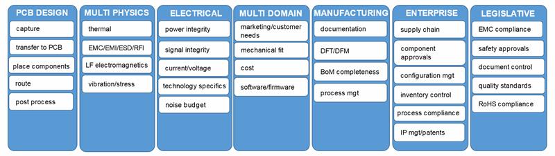
PCB design is seeing complexity grow as factors such as manufacturing enterprise requirements and legislation become relevant
An EDS conference session presented by Abaco Systems – which develops rugged embedded computing solutions – explored the same themes. Ian McCormick, design services manager, noted: “A PCB is a complex 3D puzzle with several conflicting requirements, including: component density; a restricted number of layers; signal integrity; controlled impedance; and thermal and mechanical constraints. It’s a jigsaw puzzle without a picture and only the shapes for clues. Engineers need to place components for efficient routing while satisfying mechanical, thermal and signal integrity requirements. But only one solution will satisfy all.”
Mayo agrees: “While the skills needed include knowing about placement, PCB design is also about considering many other factors. It’s not something you can teach; it has to be experienced and there is no single point of reference which can tell you what you should do.”
McCormick told the conference session: “You need a knowledge of electronics, but you also need to be artistic, creative, logical and good at problem solving.”
Abaco’s key PCB considerations
|
Mayo sees the development of a belief that, for example, modelling will fix a board design. “Lots of customers ask for simulation and signal integrity tools, for example. But are they designing to avoid the need for these?”
And things are complicated, in his opinion, with the emergence of the Internet of Things (IoT). “It has created something of a smokescreen.”
He contends the IoT cannot exist without a PCB. “Take a company designing movement sensors. They are normally passive, with proprietary connections. Now, these companies are asking whether they should do an IoT version and, in doing so, approach PCB design in the same way as any professional company would.
“But the IoT spans many sectors, including wearables. So a textile company might want to attach a PCB to a product; it’s a different range of requirements and a different group of people who want to know how to do a PCB. However, for both examples, the PCB is important.”
Mayo also believes the IoT brings the problem of scale. “The IoT device might be made in millions; volumes beyond the experience of most UK companies. That brings real business challenges.”
It also brings challenges for those companies making PCBs. “One low volume PCB manufacturer I talk to is being approached every day by companies looking for prototypes. Some are proper start ups with real ideas, some are makers, but few, if any, of them have the skills and knowledge needed to specify a PCB.”
Alongside the IoT are emerging markets: LED lighting is one example. “This market includes e-mech companies who need to come up with innovative MCU based solutions. That means a PCB and they also don’t have skills in house or the right mindset,” Mayo claims.
“But PCB manufacturers can’t afford to educate their customers and it becomes an almost self defeating problem as most PCB designs will be low volume.”
Jim Rose, a PCB layout engineer with Abaco, told the EDS Conference that PCB manufacturers can help designers to clarify their thinking. “When it comes to specifying the PCB, you need to consider board thickness and whether the design is a standard format. What’s the weight of copper, for example? Is it 17µm, 35µm or 70µm? What about the core thickness? Is it 75µm or 100µm? And what material will you use? Is it FR4 or polyimide? You have to discuss these issues with your fabricator.”
Mayo picked up this theme. “If you ask a designer what their board is made of, they’ll probably say FR4. But there are many FR4 variants, so what are they going to do; leave it to the PCB manufacturer to make a choice? FR4-200 can achieve certain results, but if you don’t know about it, then you need to.”
PCB design tools are more than capable of handling these issues, but engineers need to know how best to use them. “Altium Designer can draw 1µm traces,” Mayo points out. “But good luck in getting a PCB with 1µm traces manufactured.”
And boards are getting smaller, particularly if they’re targeted at IoT applications. “Think about a board with a BGA,” Mayo says. “It might measure 40 x 40mm, but there might be 1000 balls beneath it. How do you route those connections?”
One way, of course, is to use through hole vias to take signals to the board’s inner layers. “That works well,” Mayo says. “But if you have fast edge rates, the first thing you should be thinking about is a ground plane – and a ground plane perforated by up to 1000 vias isn’t going to work. So you have to move away from theory to the practicality of the ground plane not doing its job. Engineers tend to think about physics, but practicalities don’t always match.”
Once the decision to use a BGA package has been made, that also decides manufacturing cost and structure, Mayo notes. “Once the board is made, the opportunity to make changes is limited and the costs might be higher than you want. And if the PCB is late, that could be a ‘showstopper’.”
The solution to these and similar problems? “Designers need to get out more,” Mayo concluded. “There are exhibitions, conferences and other good sources of information out there. But companies also need to invest in proper training otherwise the issues will only get worse.”
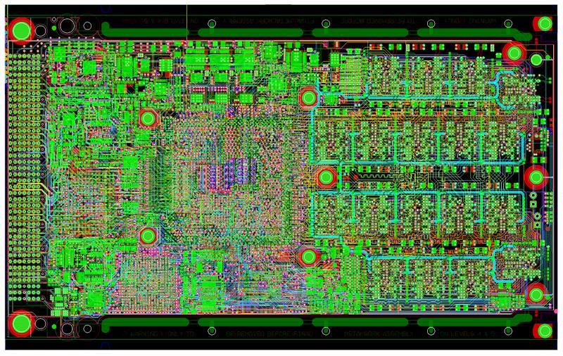
| Dealing with complexity Abaco Systems develops boards for rugged embedded applications. A recent introduction was the SBC347D, pictured above, which features:
The SBC347D – created using Mentor Graphics' Xpedition Enterprise PCB design software – was the overall winner in Mentor's 2015 Technology Leadership Awards. For more on how this board was designed, click here. |


