
Whilst you could argue that many assemblies have two or more PCBs housed in a single enclosure, a ‘multi-board system’ is very different in that it has PCBs that are soldered together, one on top of the other, as opposed to using connectors and wires to establish interconnects.
The multi-board system design practice means you can still benefit from re-use and that a range of product variants can be created through the mixing and matching of boards. Where multi-board adds extra value is through improved reliability (i.e. fewer mechanical connections to fail) and reduced manufacturing costs (i.e. fewer mechanical components needed and fewer production steps).
The boards will typically have quite different roles. For example, if you consider e-mobility - i.e. the industry trend of switching over to electric drive trains and actuation in the automotive, aerospace and other transportation sectors - many modules are multi-board systems.
Within such a module, one board will be a controller. It will probably be a high-density board and will carry BGAs and flip-chip devices, wire-bonded die and the PCB substrate may even contain structures with intentionally resistive and/or capacitive properties. It will probably feature high-speed digital and possibly even RF signals.
In this respect, the main design consideration for the controller board will be assuring signal integrity; through impedance matching and avoiding crosstalk etc.
An e-mobility module will also contain a power board for switching in and out electrical loads that might be rated at hundreds of Amps. In this respect, thermal management will be the biggest challenge. That said, the power board will also be a potential source of EMI, particularly if high currents are being sent to inductive loads. This needs to be factored into the layouts of the power and controller boards, plus the positioning of the latter on the former.
The controller board will typically be placed on the power board as if it were a large BGA device, which must be factored into the structures of both boards. We are now designing at least two PCBs at the same time. Why ‘at least’? As mentioned, product variants can be made through the mixing and matching of boards, so the controller board might be used with a few different power boards.
Above: Signal intent must be factored into the layout of the power board but if routing becomes too difficult it may be possible to revise signal allocations to both the power board’s pads and the controller board’s balls (re-routing as required)
In one place
The physical connections between the boards must align mechanically (i.e. solder bumps on the controller board and pads and on power board) and there must be no signal mismatches between the two. To ensure structural and electrical integrity there is clearly an advantage in laying out both boards concurrently and in a single canvas; which is possible in some CAD tools.
At the schematic level, connector symbols can be used to represent interfaces between the boards. These connectors initially exist as temporary components on each board and establish the electrical connectivity.
For layout purposes, it would be best to start with the controller board as it will need be ‘treated’ as if it were a single component by the power board. Having defined the controller board’s shape and size, all standard components would be placed. Most would be placed on the top side but, as mentioned, embedding (if only partially) is an option.
For connection purposes we need a component footprint on the underside of the controller board. In Zuken’s Design Force, for example, this temporary component exists initially as connection point crosses as an indication of pad (or ball, if you prefer to think BGA) positions and padstacks.
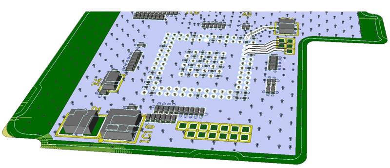
Regarding the placement of each of the pads (see Figure 2), the signals ‘intent’ must be factored in. In other words, for a signal that must connect with the power board, whilst routing from the pad of a topside component to the nearest pad on the underside might be practical for the controller board it may not be as convenient for the power board to receive the signal in that physical location. Compromises will need to be made before placement (see Figure below).
Next, the power board would be assigned a shape and dimensions. Again, all standard components would be placed. The controller board would be assigned to the temporary component of the base board schematic and subsequently placed at its intended position. As with the assigning of signals to pads on the controller board, the same considerations apply for the power board. Signal integrity must be maintained through, for example, impedance matching for high speed signals. Here, the beauty of working in a single canvas is that impedance matching can be managed for signals that transition between boards.
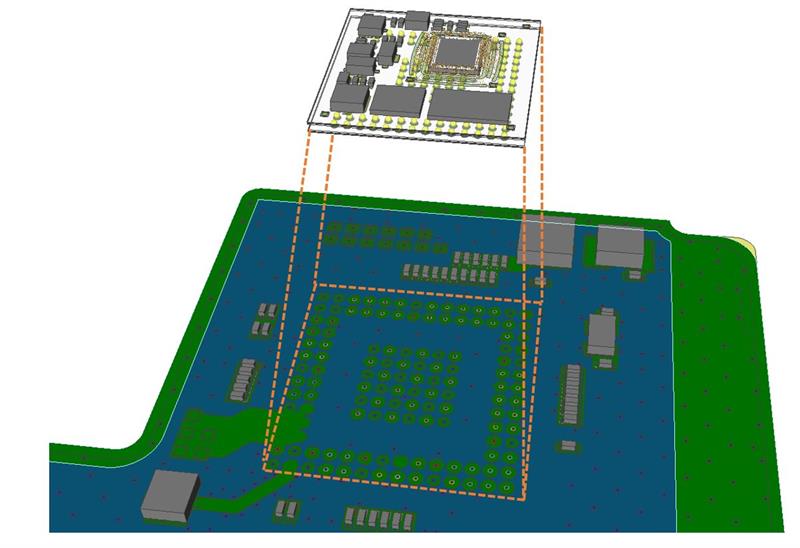
Above: The design of a multi-board system is greatly simplified when the designs exist in a single environment and the designer can see roughly where the board-to-board connections must go
Working on a single canvas also helps with the placement of power and ground grids, which are very important for the design’s overall Power Distribution Network (PDN), and the alignment (between the boards) of copper filled areas to help with thermal management (heat dissipation).
Design rule checks (DRCs) can flag any infringements, such as failing to maintain a suitable galvanic isolation distance when routing high current signals.
Accordingly, if the pad of one board is reassigned then executing an ‘update’ will keep the two design parts in sync. For example, to reduce
crosstalk it is sometimes necessary to switch the positive and negative halves of an LVDS signal over. If an LVDS signal transitions boards, any inversion needs to be made on both.
Electrical updates are not the only ones that can be easily implemented. Sometimes, it will be necessary to move one or more pads relative to the others; and we have this flexibility as the underside of the controller board and its position on the base board exist as temporary components.
It really stacks up
The benefits of designing the PCBs – at the schematic entry and board layout levels – for a multi-board module are considerable. Whether you regard the top board as a ‘component’ or as part of single board that just happens to have different design requirements (and therefore rules) is academic. The boards work together as one.
Also, it does not matter if the board technologies vary considerably. For example, if the base board of a module is to be close to a heat source – such as a combustion engine or power inverter – then it can be prototyped in FR4, be functionally verified on the bench, and then retargeted at ceramic.
The controller board would then be a forced-air-cooled component on that ceramic power board.
Author details: Herbert Ritthaler is Zuken’s Solution Architect Electronic Design


