
It’s this aspect that Mentor Graphics’ annual Technology Leadership Awards (TLA) looks to recognise. Now in its 26th year, this year’s Awards were said to have drawn the usual high quality entries, with winners selected in 12 categories. But the award for best overall design was won by a team from Abaco Systems’ Towcester facility. Between them, Jim Rose, Zeshan Hussain, Eric Mills and Peter Woodruff created a 3U VPX single board computer in 12 weeks using Mentor’s Xpedition Enterprise PCB design software. Winning the military and aerospace section was a team from BAE Systems in Rochester.
David Wiens, business development manager with Mentor’s system design division, runs the TLA competition. “Designs are smaller, denser and increasingly more complex, which means engineers are dealing with trade offs they never had to consider before, including performance, routability, placement and manufacturability.
“Over the TLA’s last 20 years, board density has increased by seven times. One of this year’s entries saw a team having to retain a product’s functionality while making it run twice as fast on a board which was one quarter the previous size.”
Ian McCormick, CAD/CAM manager at Abaco’s Towcester site, said design started in early August 2015, with the product released in late October. “Along the way, the team had to deal with multiple challenges, which meant a number of things were working against each other; all while working to a strict deadline.” An indication of the complexity is shown in the panel.
The winning product – the SBC347D – is based on an Intel Xeon D processor. It features 36 DDR4 memories and a range of communications interfaces, including PCIe Gen 3, 10Gbit Ethernet, SATA and USB. According to eCAD design engineer Jim Rose, placing the 36 DDR4 memories required some innovative layout, as well as the innovative use of single sequential and blind vias. “Nothing was auto routed,” he said. “Everything was ‘hand stitched’.”
According to McCormick, the aim is to get a working design as early as possible. “While we have a lot of expertise in designing products such as this, there is always another challenge to be dealt with; for example, routing the memories. Alongside that, signal integrity requirements become more challenging and there’s more heat to deal with.”
One thing which Abaco is confident of achieving is getting more components into the footprint. “We have always been good at this,” McCormick noted. “But the downside is that the board becomes more complex and therefore more difficult to complete.”
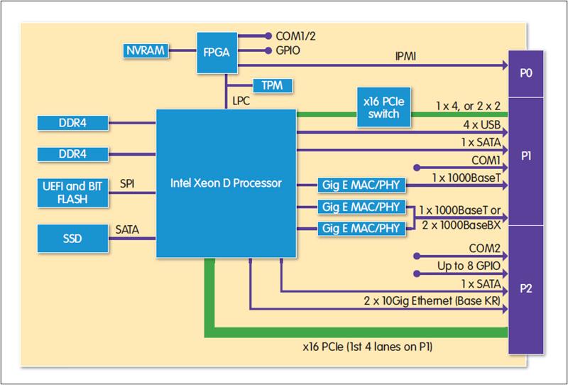 Block diagram of the SBC347D
While each Abaco design tends to start out with a ‘blank sheet’, there is a basic board template and a general outline, McCormick noted. New designs tend to be driven by the arrival of a new processor, something which can rule out design reuse. “For example, when Intel brings out a new processor, we can’t just swap out the old processor; there are questions like how the memory routing needs to be arranged and how you power the processor. If you need another power supply, you have to get that on the board.”
In the case of the SBC347D, the design needed 27 power supplies, ranging from 0.9V to 12V, with the main supply to the processor needing multiple phases to carry the required 90A.
With the design constraints faced, could the team add layers to the board? “No,” said McCormick emphatically. “Increasing the number of layers works against you in two ways. Board thickness alters the size of the vias. To plate vias successfully, the aspect ratio needs to be about 10:1; if the board is 2mm thick, you can plate 0.2mm diameter vias. But the IPC classification requires a particular size for the annular ring around the via. The larger the via, the larger the pad and the less space there is for routing.
“And if you increase the number of layers, the space has to come from somewhere as you have to stay within a product envelope.”
McCormick said the team typically designed using 18 layers. “We can’t use more than that,” he said. “Not all layers are for routing; there are power places, for example. We’ll probably use eight layers for routing.”
He noted there were various things which could be done to improve routing. “We can use sequential builds and blind and buried vias,” he continued, “but this increases cost, so we have to come up with strategies that allow the design to be completed in the most cost effective fashion.”
Design reviews along the way are essential. “We look at placement with the production people, as well as test. We consider things we need, things we’d prefer and things that would be ‘nice to have’. When the reviews are complete, you end up with something which can be assembled and tested.”
The SBC347D also features an FPGA. Rose noted the design constraints meant there was only one place for it to go – near the bottom right hand edge. “That’s not ideal as it has to connect to all areas of the board.”
There is also the issue of PCB/FPGA codesign. “So long as we followed recommendations, routing could commence by tracking near to the intended FPGA pin via,” Rose commented. “On completion of the routing phase, the pin swaps were offered to the FPGA designer and compiled into his FPGA design software using a pin swap configuration file. Once the pin swaps were acceptable, the schematic was updated and compiled, at which point, the FPGA pinout was considered locked.
“For this design, it was important to allow fluidity of the pin swap until the very end of the layout process.”
Without the option to specify more layers, the design team needed to get more on the eight layers available for routing. That means thinner traces laid out closer together. “We have to be careful in this respect because if you have controlled impedance, it becomes very hard for the PCB manufacturer to get what you want.” Currently, Abaco is using traces as thin as 0.1mm, with a similar gap between them. “You have to work with trace width to get the impedance you need,” McCormick continued, “but you can also work with materials and you need to do a lot of signal integrity work.” Rose added the team undertook a lot of signal integrity work with Intelligent Platforms, headed by renowned ‘guru’ Hany Fahmy.
Concluding, McCormick said: “We’re consistently developing our knowledge, our techniques and how to solve the problems, but we have always been good at getting more functionality into the available space.”
SBC347D statistics
Design challenges
|


