
One common challenge is interfacing components that rely on distinct communication standards, such as I2C and SPI. An I2C to SPI converter bridges this gap, enabling reliable data exchange between devices that utilise different protocols.
Here we explore the implementation of an I2C to SPI converter using the SLG47011V IC. It provides a practical approach to designing and integrating this solution, outlining key steps to ensure compatibility and flexibility in electronic system design.
GreenPAK Design
With a Memory Table, Width Converter, I2C host interface, and shift registers, the SLG47011V enables the creation of an I2C to SPI converter.
Figure 1 shows the GreenPAK design for this converter can both read and write SPI data through I2C. To write data, the Memory Table is used, which can store up to 4095 12-bit words. If you fill all 4095 12-bit words, you will no longer be able to transmit more data over SPI. The Width Converter then transform this data to MOSI SPI signal.
CNT3/DLY3 and LUT7 formed the internal oscillator, ensures writing, reading, and outputting SPI data. By default, the oscillator is set to 1 MHz, providing a stable and reliable clock source for the system. However, this frequency can be adjusted by rewriting the CNT3/DLY3 counter data via the I2C interface, providing flexibility in various applications.
For reading data, the SLG47011V uses six shift registers to store incoming SPI data. This design allows up to six bytes to be read at a time. CNT4/DLY4 and LUT5 limit the read data to six bytes, ensuring that the data is correctly read and processed. This internal limitation is important for keeping the data accurate and preventing overflow. The recording of the input data starts at the beginning. However, there is flexibility in adjusting the start of the recording by changing the counter data of CNT4/DLY4. For instance, it is possible to configure the design to start recording six bytes after the fifth byte is read.
This feature allows for precise control over data capture, accommodating various timing and sequencing requirements in complex communication scenarios.
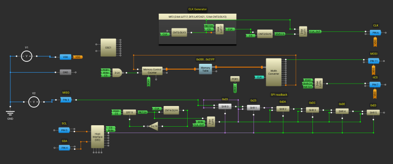
Figure 1: GreenPAK Design
Writing SPI Data
Taking a closer look at the SPI writing process. First, we need to write the value ‘0x84’ to the 0x155 register via I2C, which switches the memory table to RAM mode and makes it possible to write the data that will be sent via SPI.
The table below lists the I2C register control data which will help you to choose the correct register.
The data in the memory table is stored in registers 0x200 – 0x21FE. It is important to note that registers in the memory table are organised in 12-bit segments. For example, you can store 12 bits in the registers at address 0x200 and 0x201, and this applies similarly to each word.
So, if we need to write several 8-bit words into the memory table, the first word will be fully written into the first 12-bit segment, leaving the last 4 bits empty. The first 4 bits of the next 8-bit word will then be written into these last 4 bits of the first 12-bit segment. The remaining 4 bits of this second 8-bit word will be written into the second 12-bit segment then the third 8-bit word will be fully written to the second 12-bit segment, and so on.
As an example, if we need to send the following sequence of 8-bit words: 0xAB, 0xCD, and 0xEF you would start by writing 0xAB into the first 8 bits of register 0x200. Then, the first 4 bits of the next register, 0x201, would be used to store the first 4 bits of 0xCD. Consequently, the remaining 4 bits of 0xCD would be stored in the first 4 bits of register 0x202. The last 4 bits of register 0x202 and the first 4 bits of register 0x203 would be used to store the entirety of 0xEF.
This process of overlapping the storage of 8-bit words into 12-bit registers ensures efficient use of memory space and alignment with the chip’s data transmission protocol.
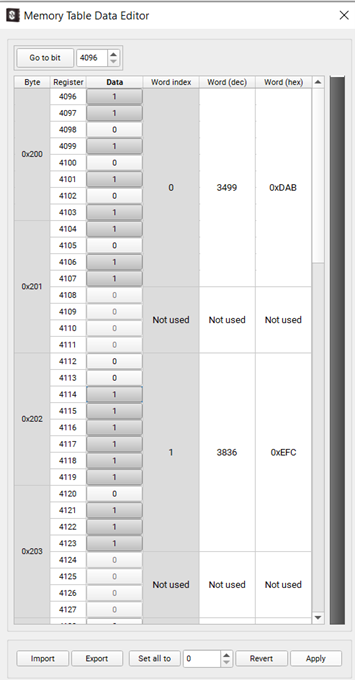
Figure 2: Example sequence of storing 8-bit words: 0xAB, 0xCD, and 0xEF in the memory table
This method of data storage requires careful attention to detail, particularly in managing the overlap between registers. Any miscalculation or oversight can lead to data corruption or misalignment, which would subsequently result in errors during data transmission over SPI. It is crucial to implement a precise algorithm for handling the writing process, ensuring that each 8-bit word is correctly partitioned and allocated to the appropriate registers without overlapping which can cause errors.
Additionally, it is beneficial to implement verification steps to check the integrity of the written data before it is transmitted via SPI. This can be achieved by reading back the data from the memory table and comparing it with the intended values. Any discrepancies can be corrected before the final transmission, which will ensure the reliability and accuracy of the data communication process.
After writing the data to the memory table, we need to write the value ‘0x8F’ to the 0x155 register. This switches the memory table to ROM mode and enables the ability to output the written data via SPI.
Finally, we write the value ‘0x03’ to the 0x61 register to set the I2C virtual inputs 0 and 1 (CS and write signal, respectively) to a HIGH level. This initiates the internal 1 MHz oscillator and begins sending SPI data via the MOSI signal.
Reading SPI Data
To read data via SPI, we must first set I2C virtual input 2 to a HIGH level and subsequently set input 0 to a HIGH level. This command set can be sent without an additional time gap between them. Once I2C virtual input 0 is set to HIGH, the internal clock starts. After 12 cycles of the internal clock, this signal reaches Pin 6, and at this point, the data read via SPI is written to the shift registers.
After 48 cycles of the internal clock, the data will no longer be written. This means any data transfer operations must be completed within this 48-cycle window to ensure data integrity. However, even after this period, the oscillator will continue to operate until I2C virtual input 0 is set to LOW.
To optimise performance, ensure that all necessary preparations are made before initiating the data transfer. This includes configuring the SPI and I2C interfaces correctly, verifying all timing requirements, and ensuring that any other system dependencies are met.
Additionally, consider implementing error-checking mechanisms to handle any potential issues that may arise during the data transfer process. This could include verifying the integrity of the data before and after transfer, monitoring the internal clock cycles to ensure proper timing, and implementing retries or error correction protocols as necessary.
By taking these precautions, we can enhance the robustness of your system and reduce the likelihood of data corruption or communication failures.
Here is an I2C command example of writing and reading the SPI data
Writing SPI data
[start] [0x08] [w] [0x00] [0x61] [0x00] [stop] //Set CS and write signal to 0, reset the shift registers.
[start] [0x08] [w] [0x01] [0x55] [0x84] [stop] //Set Memory Table to “Storage” mode
[start] [0x08] [w] [0x02] [0x00] [0xB0] [0x0B] [stop] // write the data that will be converted to SPI
[start] [0x08] [w] [0x01] [0x55] [0x8F] [stop] // Set Memory Table to “Addr to Data” mode
[start] [0x08] [w] [0x00] [0x61] [0x07] [stop] // Set CS and write signal to 1, remove reset signal from shift registers.
Reading SPI data
[start] [0x08] [w] [0x00] [0x23] [start] [0x08] [r] [xxxxxxxx] [stop] // read SHR 0 data.
[start] [0x08] [w] [0x00] [0x25] [start] [0x08] [r] [xxxxxxxx] [stop] // read SHR 1 data.
[start] [0x08] [w] [0x00] [0xDA] [start] [0x08] [r] [xxxxxxxx] [stop] // read SHR 2 data.
After reading the SPI data, the data needs to be processed.
Suppose the SPI device sends the following words: 0x02, 0x80, 0xFE, and 0x50, which are captured in the shift registers. When this data is read, we get the following results: from SHR0 (address 0x23), we read 0xE5; from SHR2 (address 0x25), 0x0F; and from SHR2 (address 0xDA), 0x28. As we can see, the SPI data is split between registers: the last 4 bits of the first SPI word (0x2) are written to the first 4 bits of SHR0, while the next 4 bits contain the first 4 bits of the next word (0x08). To retrieve the original SPI data, we need to merge the shift register data and then split it.
Results
Channel 1 (yellow/top line) – PIN# 7 (nCS).
Channel 2 (cyan line) – PIN# 6 (CLK).
Channel 3 (purple line) – PIN# 11 (MOSI).
Channel 4 (blue line) – PIN# 3 (MISO).

Figure 3. Design functionality, the process shows communication with the SPI device.
Channel 1 (orange/top line) – PIN# 4 (SDA).
Channel 2 (blue line) – PIN# 5 (SCL).
Conclusion
In summary, the SLG47011V provides a reliable and adaptable solution for I2C to SPI conversion. Its ability to store large amounts of data, adjust timing parameters, and ensure accurate data transfer supports efficient communication between these interfaces. These features make it well-suited for applications requiring precise and high-performance protocol conversion.
Author details: Andrii Velikhovskyi, Application Engineer, Renesas Electronics


