
Flash memory has made it possible to pack gigabytes of non-volatile storage into a tiny space, a factor that is making it possible to bring advanced algorithms and artificial intelligence to car navigation and driver-assistance systems and other critical applications. But flash’s rapidly increasing density can come with costs: reliability and performance.
Axel Störmann, vice president memory marketing and application engineering division at Toshiba Memory Europe, says: “By shrinking devices, makers create more sensitive products. As a result, devices are getting slower, less reliable and less robust.”
There are limits on how densely the memory cells in a 2D array can be packed, which has forced manufacturers to look at alternatives to the 1bit-per-cell architecture.
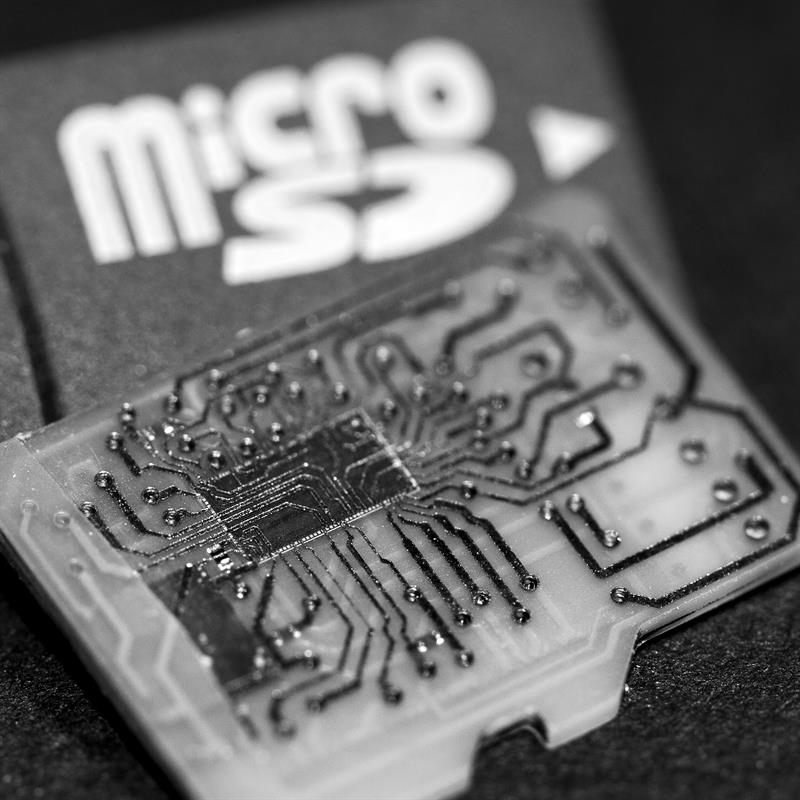
Jason Chien, product marketing manager at Silicon Motion, says: “While these advanced NAND Flash technologies enable us to store albums and photographs on a mobile phone’s microSD card memory for example, there’s a drawback when it comes to miniaturisation. There are so few electrons in each cell, that data is prone to loss through leakage, interference from neighbouring cells or from corrupted read or write operations.”
Manufacturers have looked instead to increase the number of bits they can stored in each location.
The first step was to move to multiple-level cell (MLC) designs that store two or more bits in each physical gate. But this is much more difficult to achieve reliably than with the simpler single-level cell (SLC) architecture.
Axel Mehnert, vice president of marketing at memory-controller vendor Hyperstone, says: “When reading data [from a SLC array], you measure the threshold voltage when the electrons or current can flow and interpret it as a binary value representing the data. In MLC, different amounts of electrons are ‘pushed’ per physical cell and establish multiple different threshold levels.

“The problem with this is that when measuring multiple bits per cell there is a greater likelihood of errors: the threshold needs to be measured more precisely.”
Over time, in any flash device, the process of driving electrons onto a floating gate and removing them damages the delicate interfaces. Charge traps form over time that, eventually, cause cells to become unusable. The problems become more acute with MLC because the read and write electronics are much more sensitive to the resulting variability in usage.
| “You can’t offer everything in one device. Storage systems will have be designed with application at the forefront if we are to move forwards.” - Axel Mehnert |
“If you are writing and erasing your drive a lot, it will fail more quickly,” Mehnert says.
The problem has become more apparent in recent years because of scaling. “Many manufacturers are working with nodes at, or below, 20nm and, as a consequence, the number of electrons that are associated with each bit has fallen,” explains Mehnert. “Due to production variations whether it’s temperature or some other physical effect, it’s likely that over time cells will not represent the correct state, leading to errors.”
The reliability issues could cause problems for mission-critical embedded systems. Chien points to car information systems as an example, which play a key role in driver assistance functions where the loss of a single bit of data could threaten the safety of the driver, passengers and other road users.
To address the need for reliable data storage for critical applications, a set of memory controller technologies are now being deployed in SSDs and memory arrays that are intended to be used in automotive and industrial applications.
Hyperstone and Silicon Motion have developed techniques to cater for the reduction in cell-level reliability. Such memory controllers manage the flow of data into and out of NAND Flash arrays, using features such as error checking and correction (ECC) on read and write operations to maintain data integrity.
Silicon Motion has developed end-to-end data path protection, a technique the company says can guarantee the integrity of data written to or read from an SSD.
A particular problem for the non-volatile memory in embedded systems compared to desktop systems is that some locations will receive very high write traffic as they log real-time changes, which puts a small proportion of cells under high stress.
The controller can scan for these ‘at-risk’ cells and move the data to lower-traffic regions before they fail.
“These controllers enable SSDs, based on the latest high-density TLC and 3D NAND memory arrays, to be used safely and reliably in safety-and mission-critical applications,” Chien says.
Mehnert warns that data refresh is a complex process. “Every refresh will add to the wear-down. If you over refresh you will end up destroying the flash, so you need a fairly balanced refresh strategy which is also tightly coupled to the use-case.
“For example, with read-only memory you may want to refresh in cases where the device is exposed to high temperatures or you have to scan read the whole drive to figure out where weak areas are. If you have a use-case that is very write intensive, but where the data is not stored for long, then a different refresh strategy may have to be considered.
| Above: Hyperstone’s controllers offer a turnkey platform for the industrial space and include features such as wear-levelling |
“That approach requires a lot of statistics and management of the environmental conditions when you devise a refresh strategy and it will also need to be application specific.”
Hyperstone has developed a set of algorithms which attempt to spread the wear-down evenly over a whole number of cells, so if a particular area fails, it prevents the entire system failing.
Changes to the way that flash memories are made could provide devices that are less prone to failure.

Toshiba is looking to 3D NAND structures as a possible solution. “3D NAND allows us to grow many layers on one die, which helps with the capacity issue,” Störmann explains. “The big challenge for 2D NAND is being able to address all these different demands. 3D can work around these.”
Some 3D NAND approaches form vertical strings of bits that allow tens of bits to occupy the same location on the die.
These devices are now moving into production for high-density SSDs.
| “While advanced NAND Flash technologies offer a multitude of benefits, miniaturisation isn’t without it’s drawbacks.” - Jason Chien |
According to Mehnert, newer 3D Flash architectures also comes with new failure modes: “In 3D structures, more cells are connected. If there’s a shortage or strings break, the number of cells that become defective will be significantly higher, with the result that bit errors and data loss could go beyond the ECC’s capability. If one cell breaks you can correct it using the ECC, but, if a whole block breaks, you may need something like Redundant Array of Independent Disks (RAID) to manage data redundancy and performance improvement.”
There are other approaches to making 3D NAND suitable for embedded systems.
Störmann points to through-silicon via (TSV) technology with conventional 2D NAND devices as a possible alternative.
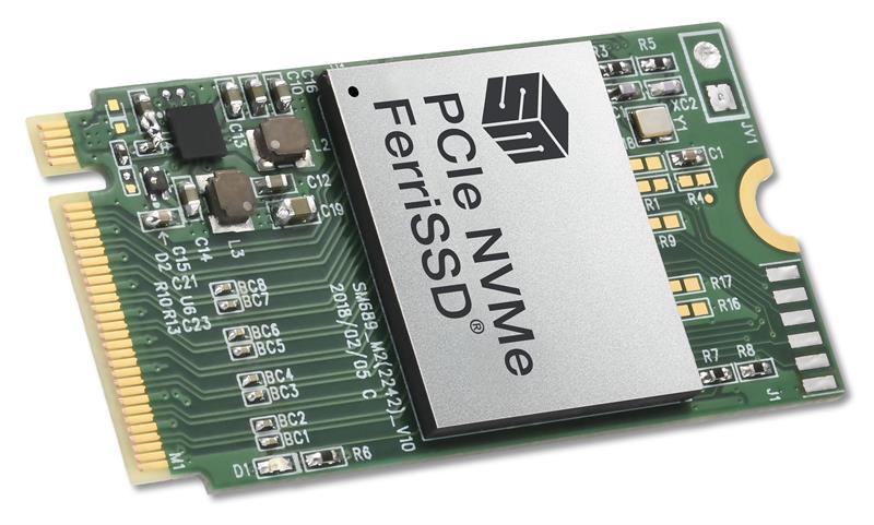
| Above: Silicon Motion includes data error detection with recovery engines to offer data integrity throughout the entire Host-to-NAND-to-Host data path |
“This is a stacking option,” he explains. “In one package you can accommodate 32 dies on one another, providing higher densities which means the capacity improves and provides quicker speeds.”
Despite the density advantages associated with 3D Flash, Mehnert believes there is still value in using 2D and that different markets will require different levels of reliability.
“We still have a lot of systems which are low capacity and very reliable. It just depends on the application,” he contends.
He insists that the only way forward when it comes to memory is to compromise.
“You can’t offer everything in one device. Storage systems will need to be more application specific and new features will require different approaches, and that will entail continuous innovation.”


