
For more than a decade, there has been little movement in clock speeds. And power savings have been made through the use of exotic materials and transistor shapes. The next step after the finFET at 7nm is some kind of nanowire or nanoribbon that is even more difficult and expensive to produce. One answer may be to think again how transistors work to find other ways to build more energy-efficient circuits.
With conventional metal-oxide semiconductor (MOS) transistors, there is a lower limit on the energy used during switching that is imposed by thermodynamics. The problem lies in the way transistors rely on thermal excitation to move enough electrons into conduction bands to operate. To generate a large enough drive current to be effective, the operating voltage needs to be significantly higher than the thermal voltage that is equivalent to the product of the Boltzmann constant and temperature. The practical limit is 60mV per decade of current increase, which is several orders of magnitude higher than the ultimate limit of computational energy determined by information theory and quantum mechanics.
One way to break the “Boltzmann Tyranny” is to move to a different type of transistor. During the 2000s, researchers looked at devices that explored side effects of quantum physics and processes that would damage conventional CMOS transistors with the tunnel-effect transistor (TFET) and impact-ionisation transistor. The TFET suffers from low drive current, which limits performance, although it has transconductance properties that may make it a good choice for ultra low-energy analogue circuits. The impact-ionisation device, as its name suggests, looks likely to suffer reliability issues. And it demands relatively high operating voltages. With either alternative, circuit designers would also be faced with the problem of coming up with topologies that are quite different to those used with CMOS.
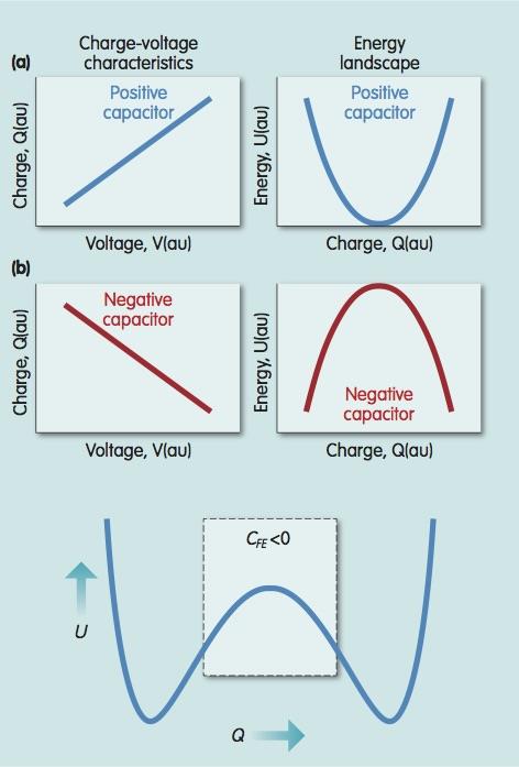
| Above: Negative capacitance. The top part of the figure highlights energy and charge, the lower, the shift that occurs in the polarisation of ferroelectric material as voltage increases |
Negative capacitance
A little over a decade ago, Sayeef Salahuddin and Supriyo Datta, then both working at Purdue University, came up with another option that would not throw away the massive design investment in CMOS. Their proposal was, at its heart, a form of circuit-design legerdemain: find a material that can introduce an effect that contradicts conventional electrical theory into the gate of the transistor. Their effect is negative capacitance.
A MOS transistor can be modelled as the combination of two capacitors in series: one is the total gate capacitance; the other is due to the semiconductor capacitance. Under normal circumstances, the combined capacitance is smaller than the value of either device. The gate voltage is divided across the two. However, if you can somehow introduce a negative capacitance into the gate electrode, the total capacitance winds up higher than the individual contributors. Not only that, the internal voltage between the gate electrode and the semiconductor capacitance turns out to be higher than the gate voltage.
With an operating voltage that is higher than the applied voltage, designers can drop the gate voltage into the sub-threshold zone but not suffer the normal consequences of higher leakage and lower switching speed. It’s a free lunch for low-power circuit design: just as long as you can find an electrical Bigfoot. It is entirely possible to measure what looks like negative capacitance, but it’s generally a side effect of inductance in a circuit with very low resistance.
Although a material that exhibits negative capacitance sounds impossible, researchers claim to have found a true negative-capacitance effect, albeit fleetingly, in ferroelectric materials.
Rather than a parabolic relationship between voltage and energy stored, the shift in polarisation that occurs in a ferroelectric material as voltage increases follows a W-shaped trajectory. It’s during the short period when polarisation begins to switch that researchers believe it is possible to exploit the negative capacitance as a form of voltage amplification. But the device needs to be stabilised in some way to stop it switching polarisation states completely and introducing unwanted hysteresis.
In this model, the negative capacitance partially cancels out the positive capacitance in the rest of the gate stack while it is switching on, with the payoff of a reduced sub-threshold swing. That could potentially take it below the current hard limit of 60mV/decade.
Ferroelectric memories
There is further good news. For decades, work on ferroelectric memories focused on materials such as lead zirconate titanate (PZT), which proved to be tricky to move into high-volume manufacture. Even today, ferroelectric memories are far from common, though Texas Instruments succeeded in embedding them into low-power microcontrollers. But there is another contender in the form of the same hafnium oxide now widely used as the high-k dielectric in CMOS since Intel introduced its 45nm process. GlobalFoundries, for example, has been among those working to develop embedded memory cores based on modified forms of hafnium dioxide. Though its ferrolectric properties are not as good as PZT, modified hafnium dioxide is good enough to demonstrate the transient negative-capacitance effect. But there is a catch that is probably independent of materials choices.
Simulations by Borna Obradovic and colleagues at Samsung Semiconductor indicate that the negative-capacitance occurs over too long a timescale to be responsible for the results claimed so far of reductions in sub-threshold swing. Their argument is that negative capacitance may prove to be useful in the design of a new generation of ferroelectric memories, but it may not be the circuit-design breakthrough it seems. The Samsung team saw effects taking place over the period of more than a microsecond. To be useful in an augmented CMOS transistor, the effect needs to take hold on picosecond timescales.
Obradovic said at the 2018 VLSI Technology Symposium, his team’s results point to the effect being unlikely to lead to a general-purpose negative-capacitance transistor (NCFET). But observers believe the idea is far from dead. There does seem to be an effect. It’s just not clear what is causing it.
One theory is that the negative capacitance effect appears when the ferroelectric starts to switch polarisations. Rather than taking place at once, tiny clusters of the opposite polarisation appear first and expand until they merge with their neighbours over the period of ten or more microseconds. However, some experiments have suggested that the negative capacitance takes hold faster than predicted by traditional models.
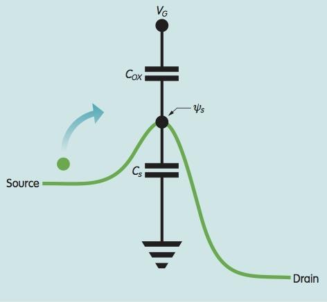
| Above: Transistor cap model |
There may be interactions in the interfaces between domains of different polarisation states that can deliver a usable NCFET. Work by UC Berkeley presented at VLSI Technology Symposium alongside Obradovic’s paper suggested experimental results followed a compact model closely enough for the model to be a reliable guide.
The UC Berkeley model suggests it could lead to transistors that work better at 0.5V to 0.6V than their pure-CMOS counterparts. But the physics looks likely to puzzle researchers for some time to come and it’s far from clear that the NCFET is ready to come to the rescue of low-power silicon chips. If it does work, scaling may return to supply voltage even as it comes to a halt in terms of device density.


