
The SubLVDS to MIPI CSI-2 Image Sensor Bridge reference design looks to provide industrial device customers with a flexible, easy-to-implement solution for connecting advanced application processors (APs) with many of the image sensors currently used in machine vision applications for industrial environments.
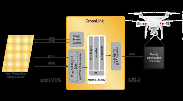
Many industrial machine vision applications use image sensors with a SubLVDS interface, which is incompatible with the MIPI CSI-2 D-PHY interface used on today’s APs. However, many industrial device OEMs want to implement these APs in existing machine vision-capable products. The Lattice SubLVDS to MIPI CSI-2 Image Sensor Bridge reference design looks to address this and lets customers quickly and easily create a bridging solution so an AP with a MIPI CSI-2 interface can connect with a SubLVDS image sensor.
“In industrial environments, customers are interested in upgrading legacy machine vision applications to take advantage of the processing capabilities and feature sets of new APs,” said Peiju Chiang, Product Marketing Manager, Lattice Semiconductor. “Rather than devote precious time and engineering resources on an extensive device redesign, the Lattice CrossLink SubLVDS to MIPI CSI-2 Image Sensor Bridge reference design provides a simple workaround that addresses legacy interface compatibility issues to get redesigned products to market quickly and cost effectively.”
The SubLVDS to MIPI CSI-2 Image Sensor Bridge reference design is free and is provided to demonstrate the use of Lattice’s popular CrossLink modular IPs, including the Pixel-to-Byte Converter, SubLVDS Image Sensor Receiver and a CSI-2/DSI D-PHY Transmitter.
Lattice also provides a complete, easy to use GUI-based FPGA design and verification software environment, Diamond design software, to simplify and accelerate device development.
Other key features include:
- 4, 6, 8, or 10 lane SubLVDS input to 1, 2, or 4 lane MIPI CSI-2 output
- Up to 1.2 Gbps bandwidth per input lane
- Up to 1.5 Gbps bandwidth per output lane
- Dynamic parameter setting via I2C
- Optional support for image cropping


