
Innoscience Technology was founded back in 2015 with the aim of creating a global energy ecosystem based on high performance, low-cost Gallium-Nitride-on-Silicon (GaN-on-Si) power solutions.
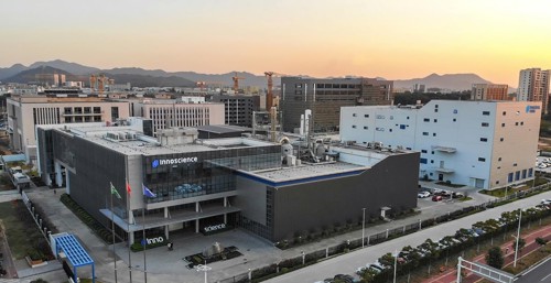
Today, the company is the largest Integrated Device Manufacturer (IDM) that is fully focused on GaN technology, and it has established two wafer fabs including the world's largest dedicated 8-inch GaN-on-Si site, featuring the very latest, advanced, high-throughput manufacturing equipment. It employs over 1400 people worldwide, with over 300 involved in research and development.
With the capacity to produce 10,000 8-inch wafers per month it is now looking to ramp up production to over 14,000 8-inch wafers per month later this year and is aiming to reach 70,000 8-inch wafers per month by 2025.
“Over the past seven years, Innoscience has developed a wide portfolio of devices from 30V to 650V and to date we have shipped more than 35 million parts for use in applications including USB PD chargers/adapters, mobile phones and LED drivers,” said Dr Denis Marcon, General Manager, Innoscience Europe, “and we have the financial backing of a number of leading industry giants such as Arm and SK Hynix.”
Innoscience produces high-performance, normally-off e-mode GaN FETs and, by introducing a stress enhancement layer, the company has significantly reduced RDS(on) without affecting other parameters including threshold voltage and leakage.
“Innoscience can design new products, provide sample devices all within
3-6 months and we can be ready for mass production within just 6 months,” says Dr Marcon.
"After several years we believe the time is right for GaN. We’ve moved from proving GaN to selling products with GaN technology inside to a point where prices are now falling. Our huge manufacturing capacity means that our customers can be assured when it comes to security of supply, which in today’s challenging climate, is uppermost in people's minds given the shortage of semiconductors."
According to Dr Marcon the fact that the company invested in 8-inch, rather than 6-inch (which is more widespread), manufacturing capabilities has given it a significant commercial advantage.
“We are the largest Integrated Device Manufacture (IDM) that’s fully
focused on GaN technology. We have the largest dedicated 8-inch GaN
-on-Si wafer manufacturing capacity in the world and we are using some of the most advanced, high-throughput 8-inch silicon manufacturing tools that are available.
“For example, Innoscience is using the latest generation of Aixtron MOCVD reactor G5+C to grow our 8-inch GaN-on-Si wafers and we have developed a proprietary 8-inch GaN-on-Si epi-buffer technology that’s been optimised for high-voltage (HV) and low-voltage (LV) devices.”
According to Macron, while there are still barriers to using GaN – cost is still an issue and customers will raise issues over the security of supply - engineers understand the benefits of using GaN-based transistors in their systems.
“They can make more efficient, more compact, lighter and even more reliable power electronic systems by using GaN-based transistors with respect to what is possible with traditional silicon devices,” Dr Marcon explained.
Unlike many of its competitors Innoscience’s proprietary technology means that it is able to supply a much broader range of high-performance GaN devices and, as a consequence, is able to address a wide range of applications and voltages (from 30V up to 650V).
“We address both ends of the market unlike many competitors who tend to have focused on one of the other. While many can deliver high voltage GaN they tend to struggle when it comes to delivering low performance devices,” added Dr Marcon.
According to figures from the research group, Yole, and quoted by Dr Marcon, Innoscience now has three times the manufacturing capacity for GaN than TSMC, for example.
“Being able to control our own fabs and by investing solely in GaN, we are well placed to manage the supply of GaN, but it’s not just about security of supply, it’s much broader than that. Our high-volume capabilities mean that we are able to offer a combination of excellent performance and reliability; extended support for GaN technology; and competitive prices,” according to Dr Marcon.
First public showcase
Earlier this year Innoscience attended PCIM, the company’s first public showcase in Europe.
According to Dr Marcon, “It proved an opportunity for us to demonstrate the huge capacity we already have and the wide portfolio of devices that we’ve developed. We were able to show off a number of designs that we’d done in partnership with specialised gate-driver companies such as Heyday and MindCet.”
Partnering with companies and engaging with the wider community has a vital role to play in helping to drive the development of a GaN ecosystem, according to Dr Marcon.
“By putting ourselves in a position to talk more about our technology and engage with customers we’ve been able to drive the use for GaN and have enabled design houses to use the technology in their solutions. By supporting them we’re able to ensure the long-term success of GaN.
“That process has meant that today we are directly supplying many leading companies and design houses who are taking our technology, packaging it and then taking those solutions to market.”
According to Dr Marcon one of the issues that has held back the adoption of GaN has been the realisation that it’s only through a significant re-design of the end product that the benefits of GaN can be truly realised.
“Many customers had thought it would involve a simple substitution of silicon for GaN, but that’s not the case,” he conceded.
“While GaN is being widely used across a number of products, if you want to benefit from using this technology you need to take a longer-term view. It does require a substantial redesign and it’s not possible to simply replace silicon with GaN - that is probably a big reason why it’s taken time for the market to reach where it has today. But, as the costs associated with GaN have fallen, so it becomes less expensive to undertake a redesign.
“People have certainly got better educated about using GaN over the past 5-6 years and at the same time have seen the real potential it offers when it comes to shrinking the size of devices and improving levels of performance. Apple, for example, is now using GaN in its chargers so this technology is now less about the future and more about the here and now.”
Innoscience recently announced the opening of a new R&D facility located in Leuven, nearby to IMEC, a centre of excellence for advance semiconductor technology, and KU Leuven, which is well known for its activities in power electronics.
“This newly established R&D centre will play an important role in improving Innoscience’s core GaN device technology and products both in terms of performance and reliability,” said Dr Marcon.
"Today, Innoscience is ready to supply the world and is 100% committed to gallium nitride. There are certainly plenty of opportunities to drive our next-generation technology, enabling power electronics designers globally and across different markets to enjoy the high performance that GaN brings. I believe we are set to revolutionise power applications as a result.”


