
As well as making a significant impact in power electronics, GaN is bringing new levels of performance to solid-state RF and microwave hardware. Many commercially available GaN amplifiers focus on providing high levels of saturated output power, but they also offer better linearity and efficiency, wider bandwidths, and lower noise, than competing technologies.
In recent years GaN amplifiers have been gaining ground over traditional vacuum tube devices such as Travelling Wave Tube Amplifiers (TWTA) in many defence and satellite communications applications, where their superior lifetime and reliability is also an advantage.
The benefits of GaN amplifiers are now starting to make their mark in telecommunications systems too, both in cellular base stations and in wireless backhaul, although the high operating voltages make them unsuitable for use in handsets. Exploiting the superior performance of GaN devices will be crucial to achieving the ambitious energy-saving targets for 5G networks as they are rolled out, particularly as the ITU is aiming for a 1000-fold improvement in energy efficiency per transported bit compared with 4G.
GaN capability
“The use of GaN technology is continuing to grow,” says Liam Devlin, CEO of Cambridge-based MMIC design house Plextek RFI. “GaN has proven capability for high power RF and microwave amplifiers, and we’re now starting to see increased availability of GaN components operating at mmWave frequencies. I believe we’ll see increasing adoption of GaN transistors in place of LDMOS for cellular base station PAs, including for 5G when these are deployed – initially in the sub-6GHz band but later in the proposed mmWave bands.”
The reason for GaN’s success is its unique physical properties, specifically the wide bandgap which is 3.4eV compared to 1.4eV for gallium arsenide (GaAs). This large bandgap gives the GaN material a high breakdown field, allowing chips to operate at much higher voltages than other semiconductor devices, and this enables them to be used in higher-power applications that would cause breakdown in other technologies. They also have a high saturation velocity, which – combined with the large charge capability – means that GaN devices can carry a much higher current density.
In a recent report, analysts Yolé Developpement forecast that by 2025 GaN will account for over 50% of the market for RF power devices above 3W, up from 20% in 2015. Although the proportion of the market belonging to GaAs RF power devices is set to drop slightly, most of this growth will occur at the expense of silicon LDMOS, which is currently widely used in cellular base stations. The size of this market – which does not include PAs in handsets and mobile terminals – was estimated by Yolé to be $1.5billion in 2016, set to grow to just over $2.5billion in 2022.
Strategy Analytics, on the other hand, values the market rather lower, but is in agreement on the growth prospects. RF GaN vendors include Wolfspeed, Infineon, MACOM, Qorvo, and Ampleon.
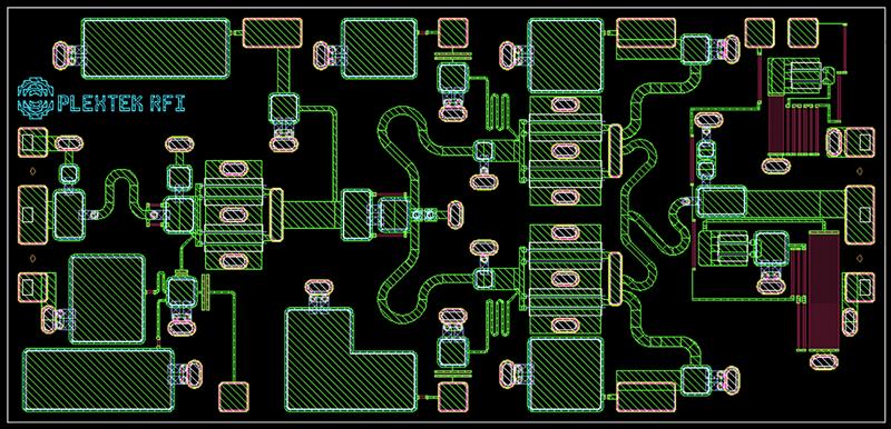 Figure 1: 15GHz GaN MMIC PA with output coupler and power detector, custom-designed by Plextek RFI for a backhaul application.
Base stations move to GaN
Infineon’s family of GaN transistors for mobile base stations was first introduced two years ago, and they were designed to build smaller, more powerful and more flexible transmitters by providing higher efficiency, improved power density and greater bandwidth than LDMOS. The wider bandwidth was not only ideal for making it easier to upgrade base stations to LTE-Advanced, where up to five 20MHz bandwidth component carriers can be aggregated to increase data throughput, but also to pave the way for the transition to 5G technology. Infineon’s figures showed the GaN devices achieving 10% higher efficiency and five times the power density of LDMOS transistors.
MACOM introduced its MAGb series of GaN power transistors in early 2016 for use in LTE macro base stations, also aiming to challenge the longstanding reign of LDMOS for that application. Boasting superior efficiency, bandwidth and power gain, but with a linearity and a price tag to match those of LDMOS, the power transistors targeted all the main cellular bands in the frequency range 1.8 GHz to 3.8 GHz. The series includes single-ended transistors providing up to 400W peak power, dual-transistors, and single-package Doherty versions with up to 700W peak power output. MACOM also pointed to a power efficiency improvement of up to 10%, and package size reduction greater than 15%, over legacy LDMOS offerings. The transistors also have a wider bandwidth – reducing the number of parts needed to cover the major cellular bands – and make it easier both to linearise with digital-pre-distortion (DPD) schemes and to implement Doherty energy-saving.
GaN-on-SiC
While MACOM’s process is GaN-on-Si, Qorvo’s recently- introduced devices – like those of Infineon – use a GaN-on-SiC (silicon carbide) process. Although pricier than GaN-on-Si, GaN-on-SiC offers superior thermal conductivity; it therefore allows higher average power levels to be handled, as well as improving efficiency and linearity. Qorvo’s asymmetric 2.5 – 2.7GHz Doherty amplifier, launched in August this year, features two pre-matched, discrete GaN-on-SiC High Electron Mobility Transistors (HEMTs) in a single package, to maximize linearity, efficiency and gain in base station designs.
Qorvo has also been the first to announce GaN devices for mmWave 5G base stations, with a 39GHz front-end module (FEM) having launched at the International Microwave Symposium in June. Other vendors are initially proposing GaAs technology for this application.
Broadband links
It is not only in base stations where GaN has the potential to boost performance. With such a dense network and high data rates, 5G will demand a rapid, massive rise in backhaul capacity, and it is likely that microwave and mmWave point-to-point links will provide most of this, since they are significantly cheaper and more convenient than fibre to install. County Durham-based Filtronic Broadband is already designing and manufacturing transceivers for backhaul applications in E-band (71 – 76GHz and 81 – 86GHz), and has described the suitability of GaN for use in this frequency band in the future. Currently their GaN subsystems are aimed at the traditional 6GHz to 11GHz long-haul radio bands, but development is planned to extend this up to mmWave frequencies.
Figure 1 above shows the chip layout of a 15GHz line-of-sight GaN PA MMIC PA with an additional output coupler and power detector, developed by Plextek RFI for a customer’s backhaul application.
UK centre of excellence
Recognising the potential of GaN has also been the main reason for the establishment by Innovate UK of the Compound Semiconductor Applications (CSA) Catapult in South Wales – an area that was already established as a centre of excellence for GaAs and GaN technologies. Although the UK no longer has an indigenous commercial fab for III-V RF devices since the sale of RFMD’s Newton Aycliffe facility four years ago, there is a thriving ecosystem of component, subsystem and system design and manufacture in this country that has compound semiconductors at its heart. The CSA Catapult aims to stimulate innovation in this area, and 5G mobile communications – along with space and defence applications – will be a clear target.
In summary, GaN not only has the ability to transform 4G networks to run more efficiently and to reduce component count, but is also likely to prove an essential enabler for the future success of 5G infrastructure and backhaul technologies.


