
The UK has a strong heritage in photonics, with academic centres of excellence around the country specialising in particular areas of the technology.
However, one of the first universities to focus specifically on photonics was the University of Strathclyde, which established the Institute of Photonics about 20 years ago.
Dr Keith Mathieson, the Institute’s director, said: “The Institute emerged from work by Professor Allister Ferguson, who was one of the first professors of photonics. He was very successful at spinning technology out from the university. For example, he established solid state laser company Microlase, which was bought out by Coherent. The Scottish operation has since grown into a big company. He also set up M Squared Lasers.
“Prof Ferguson was well versed in translating academic excellences into industrial impact and this provided the opportunity to set up the Institute of Photonics as a way of supporting the UK’s photonics industry.”
The Institute has since grown to house some 60 staff, of which 10 are principal investigators and 15 are post Doctoral researchers.
“We’re focused on three main areas of research,” Dr Mathieson noted. “Advanced laser engineering is the traditional core and, in a sense, the Institute was set up to develop solid state lasers.
“We’re also interested in photonic materials and devices, with this work led by Professor Martin Dawson. He has a strong interest in micro LEDs and has developed a strong EPSRC research portfolio.”
One of Prof Dawson’s latest projects is Ultra Parallel Visible Light Communications, or UP-VLC. The project envisions individual elements in high density LED arrays acting as discrete communications channels, as well being combined as a display, for example. The project believes it might be possible for arrays with an area of 1mm2 to transmit data at 1Tbit/s.
“The third area of interest is neurophotonics,” said Dr Mathieson. “This is an emerging area and one in which I’ve had a long term interest.” Neurophotonics, he added, emerged from biophotonics and is concerned with controlling neural circuits using light.
One particular research area which Dr Mathieson is pursuing is retinal prosthesis as a means of overcoming the effects of age related macular degeneration. “With age related macular degeneration,” he said, “the retina begins to degrade in certain areas, starting in the fovea – the central area of the retina.
“There are photoreceptors in the eye which die,” he continued. “But the rest of the eye remains healthy and people have been trying to develop devices which can capture light, translate it into an electrical signal and use that to activate healthy neurons.”
These efforts are developing electronic oriented solutions, he contended. “What happens is that near infrared light (NIR) is transmitted into the eye to provide signals – or patterns – and power to the implant. The NIR light is picked up by the implant – a silicon chip which is small enough and thin enough to be integrated into the retina.”
The chip is 1mm in diameter and completely wireless, which allows it to be tiled if necessary. “It’s about 30µm thick and features independent pixels, each of which is about 70µm in diameter – but they are getting smaller.”
Each pixel contains two photodiodes, which absorb the NIR light, turning it into an electrical signal. “Each photodiode generates about 0.5V and they are connected in series, which generates about 1V,” he said. “This stimulates the healthy inner retinal neurons and then the optical nerve.”
Each pixel also has a ground ring surrounding it, which limits how far the voltage generated by the photodiodes can spread.
The retinal prosthesis will be driven by a camera of some form, which will pick up the scene in front of the user. “The information captured will be displayed on an LDC lit by NIR light,” he explained. “If the polarisation is correct, that information will be transmitted to the back of the eye at movie frame rates and detected by the pixels in the implant.”
Dr Mathieson is working closely with Professor Daniel Palanker from Stanford University, where he was researching the topic before becoming director of Strathclyde’s Institute of Photonics. Prof Palanker’s technology has been licensed to French company Pixium Vision, which is commercialising it.
“Our aim is to verify in clinical trials that useful vision can be restored.”
And there is one simple way of verifying that: the Snelling Chart used be every optician. “The inability to detect the capital E at the top of the chart is the legal definition of blindness in the UK,” Dr Mathieson concluded. “We want to get the visually impaired back into the world of the legally sighted.”
Centre for Applied Photonics The Fraunhofer Centre for Applied Photonics (CAP) was established in 2012 in collaboration with Fraunhofer IAF and the University of Strathclyde. Fraunhofer CAP offers professional R&D services to industry and says training of PhD and EngD students is a fundamental part of its mission. Its main areas of expertise include: novel laser sources; continuous wave and pulsed laser sources; sensing and imaging systems; measurement and instrumentation; iIntegrated fibre photonics; and waveguides and plasmonics. Dr Mathieson said the collaboration has been a fantastic development “There’s about 30 people working there and, between the two of us, we have a cohort of about 100 investigators. “While the University is doing strategic research into applied photonics, the Fraunhofer Centre is serving industry’s needs by interfacing with the University. It’s a great way of getting industrial impact from academic research.” |
PolyPhotonics pursues plastic components
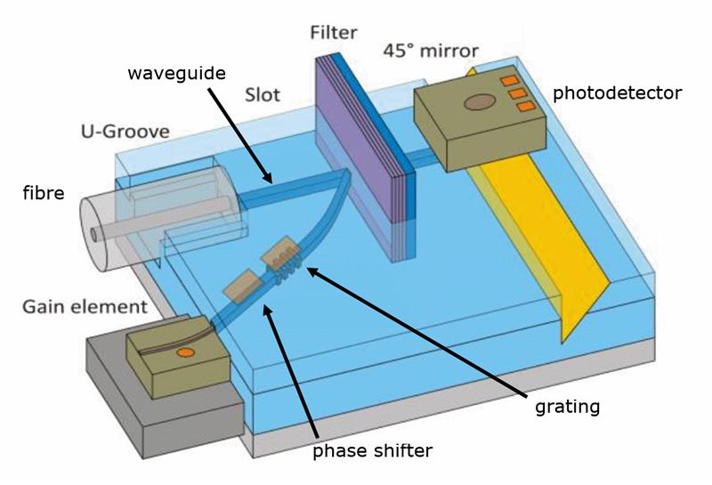
The PolyPhotonics Technology Platform provides a toolbox of hybrid optical building blocks. Using suitable technologies, members of the initiative can put these basic building blocks together to form flexible modules for integration into compact functional components. At the platform’s core is a chip featuring optical waveguides made of plastic. The chip can also feature other passive elements, including optical fibres, thin film filters and micro-optics, as well as active elements such as photodiodes or laser chips. Using micro technological procedures, the latter components are connected to the waveguide chip. An unusual element in the project is the use of a polymer for waveguide boards. This board, which might measure 1 x 5mm, is needed as a component for the socket outlet of the future (see image). Crispin Zawadzki, deputy head of polymer optoelectronic ICs Group at Fraunhofer’s Heinrich Hertz Institute, is project manager for the PolyPhotonics Network. He said: “Existing technologies can no longer handle the tidal waves of data streams. Our common research goal is the creation of very small, very potent and very low cost polymer chips.” |
 Eleven regional enterprises and three research institutes are pooling their expertise to create PolyPhotonics Berlin. For the first time, say the partners, they will be able to create comprehensive solutions using plastic optical components. Between them, the partners want to create innovative materials and methods for the production and assembly of multiple use photonic components.


