
Dr Rickman is no stranger to the world of photonics; he founded Bookham Technology in 1988 and saw the company rise to FTSE100 status. Part of Bookham’s appeal was its production of networking components based on silicon photonics technology. “We had silicon photonics in high volume production,” he noted. “Then the dot com crash came. Bookham was on the right track, but there was massive disruption.”
Since then, Dr Rickman has remained involved in the photonics industry, but has had a lower profile. Now, he has come back into the spotlight with Rockley, with solutions to the problems experienced by datacentre developers in his sights.
“I’ve looked at other efforts in silicon photonics and have seen little progress. Where Bookham had telecomms in its sights, we can see the market for datacentre technology will be bigger.”
In his opinion, the basic issue is the amount of data being handled and the speed at which it is being transmitted. “The line rate in network equipment is rising from 1G to 10G to 25G,” he said. “And the distance over which electronic signals can be driven is becoming ever shorter; there are a lot of backplane problems. I think there are opportunities to move forward with a combination of silicon photonics and CMOS technology in the same package. Rockley’s mission is to develop massively scalable photonics technology.”
The use of photonics will, he believes, bring lower cost, more compact datacentres that consume less power.
“Operators are increasing the number of servers in their datacentres,” he noted, “and these can benefit from Moore’s Law, with more compute capacity for less cost. But the network equipment has two problems. When you double the number of servers you want to connect, the amount of network equipment needed increases by a factor of six. And Moore’s Law doesn’t help this I/O problem; the more transistors you put on a chip, the more it becomes a bottleneck in terms of the number of connections you can make.”
Rockley is looking at the creation of an optimum switch architecture, with the best combination of CMOS and photonics technologies. “We want to create something that can be ‘dropped in,” he continued, “and which can scale in a linear fashion.”
He pointed to the number of layers in a network. “We’re looking to compress the number of switch layers through an innovative architecture and the introduction of photonics. If you replace electronics switching with optical switching, you don’t need to go to smaller and smaller CMOS nodes.”
In effect, Rockley is looking to build a photonic ASIC. “But it needs to have all the right features, so we are integrating silicon photonics with CMOS technology, creating a series of building blocks that don’t exist anywhere else,” said Dr Rickman.
If you were able to ‘take the top off’ of one of these devices, you’d see the CMOS element handling packet processing, while the silicon photonics content dealing with switching and transmission.
“These devices must be able to communicate within a card, a rack and across a datacentre. If you only produce a photonics device that gets data off the chip, you need to go back into the electronic domain to regenerate the signal and then return to the optical domain.
“Our approach has powerful photonics which can get anywhere and do that using less power than it takes to push a 25G signal across a couple of inches of PCB track.”
Rockley has developed its own silicon photonics process, but remains a fabless company. “We will be licencing the Rockley fabric,” Dr Rickman noted. “Within that will be things like the right protocols to allow chipsets to talk to each other.”
Despite the focus on photonics, the only overtly component in one of Rockley’s photonics ASICs is an InP laser. “We use this as the gain element,” Dr Rickman explained. “We lay it down as a bar on the silicon photonics segment; the rest of the laser circuitry is gratings generated in silicon.”
And he notes that many features are ‘MEMS like’. “We’re not competing with the feature size of modern CMOS devices; that generates bad photonics performance. We have determined the optimum size to build high performance photonics circuits.”
One of the issues he has with modern silicon photonics is feature size. “The wavelength of light used in comms is 1300 to 1500nm; roughly 100 times the wavelength of an electron. If you try to cram photons into too small a space, they behave badly, with polarisation and scattering affected by manufacturing tolerances. Dealing with this is beyond the ability of semiconductor processes.
“However,” he concluded, “we can’t do what we’re doing without having made significant progress in CMOS design, particularly in analogue and in silicon photonics.”
Photonics in space
A team of NASA engineers is building an integrated-photonics communications modem and the agency says this could ‘transform everything from telecommunications and medical imaging to advanced manufacturing’. Mike Krainak, who is leading the modem's development at NASA's Goddard Space Flight Centre, said: "The technology will simplify optical system design. It will reduce the size and power consumption of optical devices and improve reliability." The modem – which will integrate optical functions such as lasers, switches and wires – is set to be tested on board the International Space Station in 2020 as part of NASA’s Laser Communications Relay Demonstration (LCRD). The mobile phone sized device will be the first step towards embedding these functions on a chip. LCRD promises to transform the way NASA sends and receives data – until now, NASA has only used RF communications. It will use lasers to encode and transmit data up to 100 times more quickly than current communications equipment, while weighing less and consuming less power. Meanwhile, ESA engineers are developing the European Data Relay System (pictured). Normally, low orbiting satellites – LEOs – must come within view of a groundstation before they can download their information. However, by uploading data to geostationary satellites via laser, data can be sent to Earth in almost in real time. The system will use laser communications to allow LEOs to send data to geostationary satellites at rates of up to 1.8Gbit/s. According to ESA, about 1W of optical transmission power is needed to achieve stable links between LEOs and geostationary satellites over distances of 45,000km. |
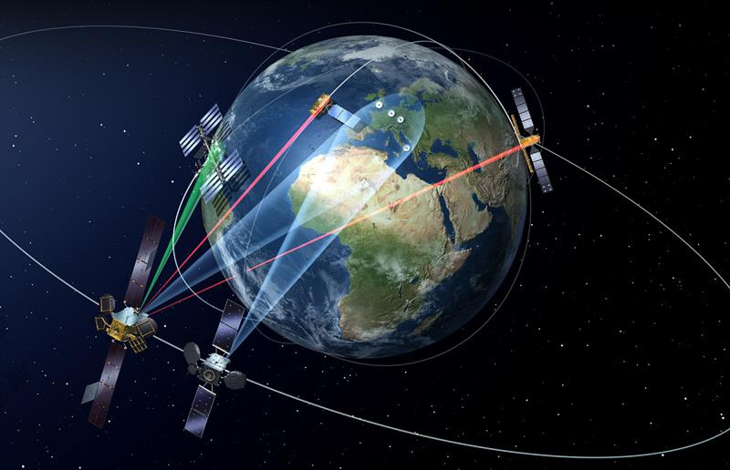 Both NASA and the European Space Agency (ESA) are looking to use photonics to boost the communications ability of their satellites.


