
According to Professor Otto Muskens, principal investigator in the University of Southampton’s quantum light and matter group, pictured, demand for optical interconnect is growing from the data centre world. “Intel is just one of the companies developing applications where silicon photonics can replace copper wires and interface with optical fibre. And, because silicon photonics is coming closer to boards, there is the need to develop integrated solutions.”
In Prof Muskens’ view, there are a lot of potential applications for such products, including low cost sensors for use in the IoT. “These will need low cost photonics interfaces,” he contended, “and that’s where silicon photonics will have potential.”
And he says the ‘basic toolkit’ is well developed. “At the engineering level, we’re at the conceptual stage, seeing if we can integrate new kinds of physics.
“There’s a huge worldwide investment in photonics and the technology is being pushed towards the wider market. But there are still questions about how of this technology can be silicon. Other options include III-V materials.”
And one of the questions being discussed in companies and academia alike is just how far photonics and optoelectronics can push into the world dominated by silicon. For example, will photonics stop at the interface, rather than becoming part of the computing platform?
“I think that might be the case,” said Prof Muskens, “but there is the discussion. The problem is that the performance of many electronics elements is so good that it will be very difficult to replace silicon. Nevertheless, while photonics will be used at the interface to transport information, there is a push towards all optical data processing.”
A quick look through the news pages of New Electronics shows that much research is underway into optoelectronics, with some teams looking to exploit the properties of graphene and other 2D materials.
There are a number of reasons why the optical domain is preferred for certain applications. In data transfer, for example, it’s much faster to use light. But the downside is that data has to be converted between the domains and this brings conversion losses.
“You’re going to lose energy going from the electrical to optical domains and back again,” Prof Muskens pointed out. “If you can make a data transport system all optical, that will be good, but it will be limited by the availability of components for switching.”
And it’s this issue which Prof Muskens and his team are examining closely. “We’re looking at whether we can make a router that can switch light going across a chip in an optical network. The idea is for light to be moved from A to B, but in a flexible manner. Our target is a universal element that can be programmed to handle light.”

According to Prof Muskens, other teams are addressing the question, but their approaches are based on interferometers. “These are bulky,” he pointed out. “We’re trying to develop more compact solutions in which you can generate patterns of light and project them onto a chip.”
Working with researchers from the Institut d’Optique in Bordeaux, the Southampton team says it applied the concept of spatial light modulation to the problem and devised a new way to control light in a chip.
The approach uses multimode interference (MMI) devices, which are said to enable the splitting and recombination of signals. Interplay between the many modes travelling through the MMI can be controlled dynamically, with a pattern of perturbations effectively shaping the transmitted light. This is said to allow light to be routed freely in a static silicon element and could therefore act as a building block for field programmable photonics.
Researcher Roman Bruck, lead author from the University of Southampton and currently working at Luxtera, a leading developer of silicon photonics for data centre applications, noted: “We have demonstrated a very general approach to beam shaping on a chip that provides a range of useful functionalities to integrated circuits. The integrated spatial light modulator turns conventional silicon photonics components into versatile reconfigurable elements.”
Conceptually, the approach is said to be similar to that taken by Texas Instruments’ DLP technology. In this, individually addressable digital micromirrors are used to direct light. “A spatial converter is something like DLP technology in that every mirror can be controlled,” Prof Muskens said. “A 2D analogue is a line array of mirrors which can send light in different directions. Our solution with patterns of light is somewhat more complicated; it could be considered as something like a hologram to direct the light. But the nice thing is that it’s flexible.”
Practical applications of the technology could include all-optical reconfigurable routers, ultrafast optical modulators and switches for optical networks and microwave photonic circuits, as well as wafer-scale optical testing of photonic chips.
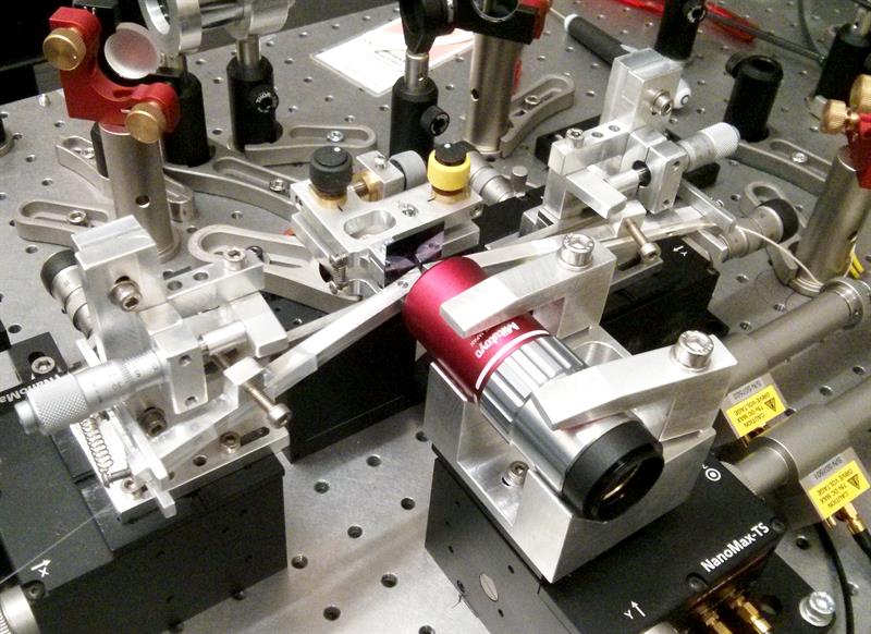
The wave shaping experiment, with end fire incoupling into the waveguide
“In principle,” Prof Muskens continued, “we could construct devices with 100 inputs and 100 outputs, routing data from any input to any output. We might be able to use a look up table approach and tune a device for each input and output. We could then program such a device in real time.”
Prof Muskens thinks that light can be used to demonstrate a proof of principle, after which technology similar to DLP could be integrated on a chip. “But we could also use a technology like liquid crystals.”
A by product of the team’s work could result in novel optical storage devices. “We’re also looking at whether phase change technology could be used to make optical memories,” he said, adding, “we’re working at the fundamental level.”
But it might also be possible to take the approach in another – potentially disruptive – direction. “Another approach could be to make a universal design and, depending on the application, configure the chip for that particular application,” Prof Muskens said. Step forward the optical FPGA.
“In theory, you could create an array in which you could program functionality. It’s a bit like science fiction at the moment, but it’s the goal and this could be an optical FPGA.”
He said there are already applications where this might prove of interest, including RF and microwave, where there is the need to interface photonics with microwaves, but with a need for flexibility. “These concepts have been demonstrated and could potentially offer a more competitive approach.”
Prof Muskens concluded: “There are many new directions to explore – from gaining a deeper understanding to application of the new concepts into real world devices. This is a potentially disruptive new approach toward field programmable chips which can enhance and complement existing strategies, or even partially replace current technology.”


