
Though increases in wafer size were originally a key part of the learning curve that drives Moore’s Law, each step up in diameter has come with an increasingly high cost, not just because it involves the building of a new clean room but because of the higher capital cost of the production equipment. Each transition has led to chipmakers falling away and seeking the help of external foundries.
Though Europe’s share of advanced manufacturing had dwindled to near zero by 2013 and the continent held less than 10 per cent of overall global fab capacity, Neelie Kroes, then commissioner for competition at the European Commission, and colleagues, recognised a shift to 450mm wafers could provide an opportunity to reverse the decline.
There were several obstacles to making it happen, not least the reluctance of local suppliers to buy their way back into direct production having outsourced many of their offerings to TSMC and other predominantly far-Eastern foundries. For the so-called Airbus of Chips to work, it needed an offshore supplier from a very short list of possible contenders and only one of which had an extensive international manufacturing network: Intel. Samsung and TSMC have operated fabs outside South Korea and Taiwan, respectively. But they were comparatively small whereas Intel’s Ireland and Israel fabs have taken turns to implement the PC giant’s more advanced processes.
In the end, the high cost of developing 450mm-compatible equipment dealt a fatal blow to plans for transition even though Intel, in particular, had pushed for the change. A decade later, the idea of moving to 450mm still seems a distant prospect and in Europe in particular production has dwindled.
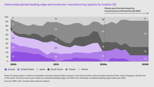
Europe’s share of leading-edge production dropped from 19 per cent in 2000 to practically zero by 2020, according to management consulting firm Kearney. And by the end of 2021, Europe’s share of worldwide integrated circuit wafer capacity overall had fallen to just 5 per cent, according to Knometa Research, about half that of the Americas and below a quarter of South Korea and Taiwan apiece.
At the same time, the supply crunch precipitated by the Covid pandemic coupled with concerns over an increasingly belligerent China put a renewed emphasis on more localised production.
Early in May, at a ground-breaking ceremony for an 300mm fab for power products being built for Infineon in Dresden, European Commission president Ursula von der Leyen pointed to tensions between China and Taiwan possibly reaching a point where they “do immediate and serious harm to Europe’s industrial base and our internal market”.
Other investments in the EU include a significant expansion of STMicroelectronics’ 300mm capacity for silicon-on-insulator CMOS in Crolles, France in a joint venture with GlobalFoundries together, following the opening of another 300mm fab for mixed-signal and power devices in Agrate, Italy that the chipmaker shares with Israeli foundry Tower Semiconductor.
Focus on Germany
But Germany is the main target for several large chipmaking plants. US-based Wolfspeed has agreed to construct another automotive-focused plant with the German subsystems specialist ZF. And TSMC is considering its own joint venture, again for automotive ICs, in Germany. According to comments from senior vice president Kevin Zhang at the foundry’s European technology symposium in late May, an announcement would have to wait for a company-board meeting in August.
The most expensive fab is likely to be Intel’s in Magdeburg: estimated to cost €12bn more than the €5bn of Infineon’s power-semiconductor facility. But with plans to make sub-2nm devices this would help deliver the kind of production that EU politicians would like to have as demand for advanced nodes increases.
According to Kearney’s report, consumption of leading-edge devices could quadruple between 2020 and 2030. At the technology symposium organised by Imec, which is responsible for much of the advanced R&D needed for these future nodes, Thierry Bretton said, “We are refusing any attempt of geographical segmentation where Europe would produce mature nodes while Asia and the US would produce advanced nodes,” he said.
To get Intel’s fab in Europe, the public price tag so far is a little under €7bn though reports in German newspapers have indicated that higher energy prices have convinced Intel to try to seek a subsidy closer to €10bn. One option may be to avoid direct spending and instead provide the chipmaker with energy from a dedicated renewable-energy farm that could deliver the huge amounts of electricity needed by the EUV lithographic scanners Intel expects to operate there.
Across the Atlantic, Intel is likely to command a lower subsidy as the federal funds in the CHIPS Act passed last year are capped at 25 per cent of the cost, though residents of Ohio where the company plans to build two fabs of a similar kind to the one at Magdeburg are expected to contribute an additional $2bn. However, the extent of the subsidy is made less clear by the inclusion of clauses in the act that let the government collect a share of revenue from profits that exceed a threshold agreed between the chipmaker and the US government.
Before the CHIPS Act passed, TSMC opted to build a sizeable installation in Arizona, and which will combine a front-end, leading-edge fab with packaging for 2.5DIC and 3DIC modules that the US wants for defence programmes as well as commercial use. TSMC’s involvement has increased since. Speaking at an event organised by the Center for Strategic and International Studies in May, Mark Kelly, US senator for Arizona, claimed, “Thanks to the passage of the CHIPS Act, their investment in our country has now gone from $12bn to $40bn. It is, perhaps, one of the biggest foreign investments in manufacturing in the history of the United States.”
Smaller buildouts
Smaller buildouts are also on the way. SkyWater Technology, formerly Cypress Semiconductor’s manufacturing operation, is partnering with Purdue University for a $1.8bn foundry in Indiana that is expected to provide customisable modules based on mature processes node. GlobalFoundries is spending $1bn on additional capacity at its upstate New York campus.
The purchaser of much of IBM’s semiconductor operation eight years ago, GlobalFoundries has, in turn, filed a lawsuit about the help provided by the computing giant to a project that aims to bring Japan back into leading-edge production with a fab that will be operated by Rapidus, a new supplier backed by eight major Japanese corporations.
Rapidus plans to start production of a 2nm process that relies on a nanosheet gate-all-around transistor developed by IBM researchers. Japan has so far pledged around $2bn in subsidies for a plant that may require a total investment of more than $35bn. The Rapidus construction is part of a larger programme of collaboration between the US and Japan to set up the Leading-edge Semiconductor Technology Centre in the Asian country. Japan also signed an R&D deal covering semiconductors with the UK in May.
Despite the heavy subsidies going into advanced chipmaking in these three key regions, the various national governments involved in these projects have taken the view that no single region will ever be self-sufficient in semiconductors. The best they can do is build up some local capacity and expertise and then use those as leverage in wider deals to secure supplies in times of shortage.
The UK’s recently published National Semiconductor Strategy, with its far more restricted funding, has similarly underlined the importance of international connections in putting together plans to streamline how supply chains are managed across industry.
Though the industry seems to be deglobalising, there is only so far the semiconductor world can go.


