
That’s one challenge; designers are also trying to anticipate the expansion of features within existing hardware, as well as making their products capable of being upgraded when new technology becomes available.
Given that costs must be kept low in most instances, expensive connectors and complete board swaps are not the way forward, so what should designers be thinking about when it comes to designing PCBs for IoT applications?
Multiple boards
Distributing the electronics among several PCBs is one solution to most of the challenges associated with IoT devices. From a mechanical perspective, multiple boards allow the electronics package to fit into ‘unconventional’ spaces. Products such as wearable devices, controls at manufacturing plants and safety and control devices deployed in a vehicle all may need to fit the available space. Figure 1 shows a typical IoT device with its electronics distributed over several boards, which are then folded together for final assembly.
In other applications, the electronics must fit into an existing package that may not have been designed to house additional components, so integrating them, as well as finding power, can be a challenge.
In this case, rigid-flex PCB components is a potential solution, with designs looking to fit multiple boards into unusual spaces.
In Figure 2, designers were challenged to add Bluetooth capability to a heart pump so that it could be connected to the Internet for remote monitoring. After searching for space to contain the circuitry, they found unused space in the connector. As a result, they designed small rigid boards connected by flex circuitry to make the necessary components fit, with a short flex segment fitting over the existing pins to tap into power.
While some applications will use multiple rigid boards in traditional ways, techniques such as 3D PCBs, mother/daughter boards and – soon – 3D printing techniques will be necessary to make designs fit into constrained spaces. Other applications will require a combination of rigid and flex.
One area that relies heavily on rigid-flex technology is wearable IoT devices, which must not only be small and lightweight, but also have to adapt to go and cope with the user’s movements. Designers can not only use flexible circuitry to conduct signals, but also to allow the entire package to flex while not breaking, shorting out or being uncomfortable to wear.
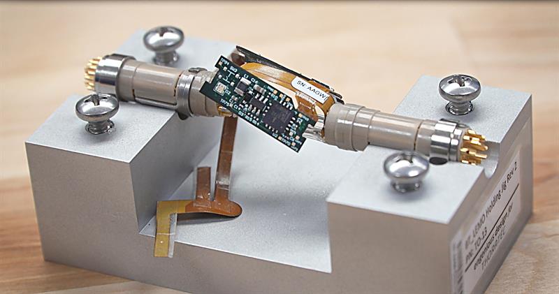 Clever solutions, like fitting Bluetooth communications inside a connector, will be necessary in future (Pic: Engenious)
However, rigid-flex designs are challenging and their development can be assisted with 3D modelling, now found in many design tools. Being able to view multiple boards in place in the enclosure helps to eliminate problems such as clearance issues. Not only is 3D visualisation critical for ensuring that the finished PCB will fit into the package, but full-motion 3D simulation views also help the designer to clearly communicate the assembly to manufacturing. In the case of wearables, the 3D simulation has been used by designers to model movement exactly and how the rigid-flex circuitry flexes with that movement.
Future expansion
Product evolution is inevitable if designs are to offer better functionality and to take advantage of better technology. Building on experience, designers are now incorporating ways to allow products to be updated without rendering legacy versions obsolete.
Expansion is twofold: expanded features and functions, and expanded technology.
 Full motion 3D visualisation allows designers to better communicate to manufacturing how products are assembled
Features and functions: Features and functions are often updated on products as new uses, apps and requirements appear. Increasingly, features and functions are added via software updates – and this is important for IoT devices, since many will be difficult to access.
It is already common for phones, tablets and similar devices to receive regular updates via the internet or mobile network. For IoT devices that operate wirelessly, updates that add features and functions will be applied via over the air (OTA) updates. This approach may require hardware security and additional PCB layout considerations to prevent hacking.
Adding some features or functions may require hardware updates. Here, designers must consider the possibility that a port or connector might be changed in the future and look to make that process as painless and quick as possible. Other techniques, such as leaving areas of the PCB unpopulated for future updates, have been used for some time.
Technology Updates: In the future, we are likely to become reliant upon many IoT devices and will expect them to evolve with technology and to be capable of being updated in a relatively convenient and inexpensive way.
The trivial solution – but also likely to be most expensive – would be to swap out the entire device. More palatable solutions would look at swapping out the updated components. To support this, designers must be ore conscious of development trends and component manufacturers more conscious of easy-to-perform upgrades.
With multiple-board solutions, the technology more likely to be updated could be isolated to a particular board and that could be made more accessible. For example, the processor and memory could be considered most likely to be upgraded and confined to one board. Considering how and what might be upgraded in the future will become a more common PCB design issue.
Many boards, little space
The near future for IoT devices with respect to PCB design is clear: circuit complexity and speed will continue to increase, while the space available for the electronics diminishes. For most IoT devices, the solution is likely to include electronics distributed across multiple boards, often employing flex circuitry to make it all fit. Meanwhile, designer will need to take advantage of 3D visualisation tools in order to create imaginative solutions.
Fortunately, these tools and design methodologies are fast becoming part of the mainstream because, without them, IoT designs are likely to present insurmountable challenges.
Author profile:
Mark Forbes is director of marketing content for Altium


