
That failure rate, however, is not across all sectors. This is most likely because of stringent regulations in some sectors, such as medical and aerospace, or because the products being developed are to join a product line that has historically been designed with EMC in mind. For instance, mobile phone developers live and breathe wireless connectivity and are well versed in minimising the risk of unwanted radiations.

Those most falling foul of EMC issues are the designers of PCBs intended for white goods - such as toasters, fridges and washing machines – which are joining the plethora of internet-enabled devices connected wirelessly to the IoT. Also, because of the potentially high volumes involved, re-spinning PCBs can introduce product launch delays. Worse still, product recalls could be very damaging to the company’s reputation and finances.
| "It's always best to design with EMC in mind, rather than risk re-spins." Ralf Brüning |
Where’s noise coming from?
There is no shortage of guidance on designing with EMC in mind, and many companies have their own in-house PCB design and EMC rules. Guidance can also come from external sources, such as legislative bodies, IC vendors and customers. However, accepting all guidelines at face value can lead to an over-defensive EMC strategy, and introduce project delays. Rules should be evaluated individually to determine if they apply to the current design.
That said, your basic, common sense rules will always apply. For instance, to supress noise sources on a PCB you should:
• Keep clock frequencies as low as possible and rising edges as slow as possible (within the scope of the requirements spec’);
• Place the clock circuit at the centre of the board unless the clock must also leave the board (in which case place it close to the relevant connector);
• Mount clock crystals flush with the board and ground them;
• Keep clock loop areas as small as possible;
• Locate I/O drivers near to the point at which the signals enter/leave the board; and
• Filter all signals entering the board.
While the above measures will help mitigate against some of the most common EMI issues, every powered PCB will still radiate EM energy. This is because every current produces a magnetic field and every charge causes an electric field. The total radiation will be the sum of signal loop differential-mode radiation, common-mode radiation (both voltage- and current-driven) and radiation produced by the Power Distribution System (PDS).
Looking at these in more detail
• Differential mode radiation is caused by transmission line loops, and the signals creating differential currents (see Figure 1). Countermeasures include using shielded layers (Vcc or Ground), placing critical signals on inner layers (also known as striplining), avoiding long parallel runs for signals and, as mentioned above, minimising the loop area and keeping signal rise and fall times as slow as possible.
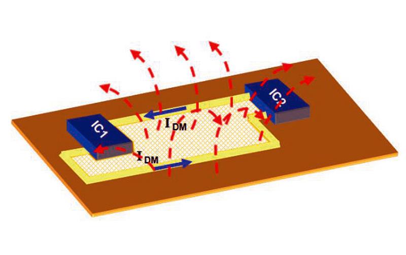
| Figure 1: Differential mode radiation |
• Common mode radiation is often the more critical EMC design aspect as the EMI is more ‘visible’ in the far field. It is created from parasitic currents (for example, switching currents or inducted currents by flux couplings) or parasitic voltages (such as crosstalk voltages to active IO-signals). The countermeasures include removing the sources of those parasitic currents and voltages - hence avoiding crosstalk between fast-switching signals – and smarter component placement and routing to avoid flux coupling and wrapping effects.
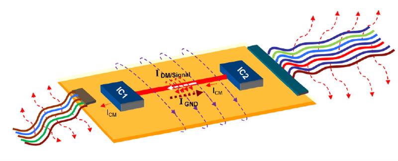
| Figure 2: Common mode radiation |
• As for PDS, it can radiate because the PCB is essentially an LCR resonator, comprising inductive elements (the tracks), capacitance (ground and voltage planes are like the plates of a capacitor) and resistance. Countermeasures for PDS EMI include lowering the board impedance, avoiding inductance and ensuring sufficient decoupling.
In addition, ICs are also a source of EMI and will contribute to the PCB’s EM profile. This must be factored in during IC selection, and chip vendors should be able to provide you with information on the EMI behaviour of the circuits.
Rule checkers and simulations
Many PCB design tools include EMC rule checkers. Checks include looking at the design data geometry for instances where signal crosstalk may occur (because of parallel-routed traces), instances of little or no shielding, and where decoupling may be required.
The rules will incorporate the ‘know-how’ of many EMC engineers. However, it is important to know their origin and how they were implemented by the CAD tool vendor; and you are in your rights to ask to see the vendor’s rule books. The tools should also allow you to highlight PCB areas where EMI suppression and EMC integrity are key – you tell the tool what your priorities are.
But let’s not forget, these are post-layout checks. It is always best to design with EMI and EMC in mind rather than embark on a trial-and-error exercise. Also, you will receive little if any steer on what the EM radiation levels are likely to be.
For a more advanced analysis, simulation is required. As with EMC design rule checkers, the meaningfulness and therefore value of the results will depend on how well the digital representations of the board and its behaviour have been rendered, plus of course how well the variety of EM equations have been implemented as software algorithms. Again, the tool vendors should be able to supply information. You should also take some representative measurements to validate the simulation methodology, and compile metrics to act as the basis for interpreting future results.
There are many numerical 3D EM simulation tools on the market, some of which are dedicated to specific activities such as antenna design. They are well-suited to what-if studies and the optimisation of structures. They can model all EMI effects for a given structure, but they do require considerable computation power (memory and CPU time) and tend to cost a lot. In addition, an in-depth understanding of EMI is needed to understand the results, as it can sometimes be difficult to explain using 3D EM results alone the reason for a particular radiation peak, for example.
However, for the types of PCBs used in white goods, we are not seeking to optimise antenna structures or produce a particular RF profile; we simply wish to verify that the board design exhibits good EMC – and a PCB design CAD tool with good EMC rule checkers will suffice.
Designing out EMI
While there is no silver bullet to EMC, good design work should include the identification of parasitic EMI antennas, such as electric and magnetic dipoles. Also, identify the current paths, as current flows in loops and will always look for the path of least resistance. Accordingly, plan for a proper return path (noting that ‘ground’ is not an accepted technical term in EMC engineering) and avoid crossing splits/gaps (even for differential pairs) and return path discontinuities (see Figure 3).
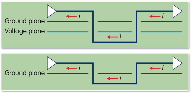
Figure 3: In the top diagram, the reference layer changes from the ground plane to the voltage plane for part of the trace. This creates an EMI antenna. Keeping with the same reference plane, as in the bottom diagram, avoids/reduces return path discontinuities. |
In summary, it’s always best to design with EMC in mind, rather than risk board re-spins, but you must have a clear understanding of which EMC rules will apply to your project. Also, having an EMC analysis capability embedded within the PCB design CAD tool can greatly reduce the risk of EMC compliance failure once the board is manufactured; but make sure the tool’s rule checker is based on well-documented and verified EMC principles and explanations. And never simulate unless a) you trust the simulator and b) you have a feel for what the results will be.
Author profile:
Ralf Brüning is product manager and senior consultant with Zuken


