The results demonstrate the potential of both III-V-on-Si and GaN-on-Si as CMOS-compatible technologies for enabling RF front-end modules for beyond 5G applications and were presented at last year’s IEDM conference (Dec 2019, San Francisco).
In wireless communication there is a push towards higher operating frequencies, moving from the congested sub-6GHz bands towards mm-wave bands (and beyond). The introduction of these mm-wave bands will have a significant impact on the overall 5G network infrastructure and on mobile devices.
For mobile services and Fixed Wireless Access (FWA), this is likely to translate into increasingly complex front-end modules that send the signal to and from the antenna. To be able to operate at mm-wave frequencies, the RF front-end modules will have to combine high speed (enabling data rates of 10Gbps and beyond) with mcuh high output power.
In addition, their implementation in mobile handsets puts high demands on their form factor and power efficiency.
Beyond 5G, these requirements can no longer be achieved, even with today’s most advanced RF front-end modules that typically rely on a variety of different technologies amongst others GaAs-based HBTs for the power amplifiers – grown on small and expensive GaAs substrates.
"To enable the next-generation RF front-end modules beyond 5G, imec is looking at CMOS-compatible III-V-on-Si technology”, said Nadine Collaert, program director at imec. “Imec is looking into co-integration of front-end components (such as power amplifiers and switches) with other CMOS-based circuits (such as control circuitry or transceiver technology), to reduce cost and form factor, and enabling new hybrid circuit topologies to address performance and efficiency.
"Imec is exploring two different routes: Firstly, Indium Phosphide (InP)on Si, targeting mm-wave and frequencies above 100GHz (future 6G applications) and, secondly, GaN-based devices on Si, targeting (in a first phase) the lower mm-wave bands and addressing applications in need of high power densities.
"For both routes, we have now obtained first functional devices with promising performance characteristics, and we identified ways to further enhance their operating frequencies.”
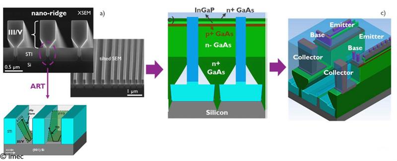
Functional GaAs/InGaP HBT devices grown on 300mm Si have been demonstrated as a first step towards the enablement of InP-based devices. A defect-free device stack with below 3x106cm-2 threading dislocation density was obtained by using imec’s III-V nano-ridge