
Speaking to New Electronics in 2016, Geoff Lees, general manager of NXP’s MCU business, said: “An increasing number of customers want more SRAM, rather than more flash and it’s now possible to imagine a system which doesn’t need external SDRAM. Non volatile memory can now be used for program memory and as a secure memory.”
A number of approaches are being considered for embedded memory on leading edge processes, but one which appears to be a strong contender is magnetic RAM, MRAM. One of the leading developers of MRAM technology is Everspin, which was spun out of Freescale in 2008.
Chief executive Phill LoPresti said: “MRAM has been around for some time now and there have been a couple of significant breakthroughs.”
Everspin’s ‘generation 1’ approach was a so called ‘toggle memory’ and used a field switching design. “Although we’ve shipped 60million units into applications such as automotive, there is a density limitation,” LoPresti explained. “Because it’s field switched, you can’t reduce the switching current and so it’s hard to increase the density.” But it was suited to use as an embedded memory, particularly in automotive applications.
And NXP is likely to be introducing products featuring embedded MRAM in 2019, said Lees. “Integration of MRAM is easier,” he asserted, “and p-MTJs are a back end process.”
Nevertheless, Lees doesn’t see MRAM as a flash replacement. “We’ll be exploring use cases that aren’t full flash or full SRAM,” he added.
Everspin has made its ST-MRAM technology available in standalone memory devices, but it will also be available as an embedded memory through Globalfoundries, which will offer the eMRAM technology as part of its FD-SOI based 22FDX process. According to the foundry, eMRAM technology can not only be used as a flash replacement for code storage, but also as a working memory instead of SRAM.
Gregg Bartlett, senior vice president of Globalfoundries’ CMOS Platforms Business Unit, said: “The introduction of 22FDX eMRAM enables system designers with new capabilities, allowing them to build greater functionality into their MCUs and SoCs, while enhancing performance and power efficiency.”
LoPresti sees the arrangement with Globalfoundries as important and noted Everspin had been working with the foundry since 2014. “We had to find a partner that could see the benefit of the technology and needed this partnership in order to deliver the memory on 300mm wafers.
“It’s all about convincing customers that you can produce ST-MRAM,” he continued. “Globalfoundries can show that it’s building MRAM for volume users.”
Renesas, meanwhile, says it has determined that its SG-MONOS flash memory will be able to be integrated into a fin structure based logic process at the 16nm node and beyond. The approach, which uses high dielectric gate insulators and metal gate electrodes, could enable the creation of on chip memories capable of storing 100Mbyte of data. With such levels of on chip storage, it says that it will be possible to create ‘highly reliable’ MCUs with more than four times the processing performance of devices made on a 28nm process.
The MONOS approach features a memory cell comprising three layers – oxide, nitride and oxide – on a silicon base, with a metal control gate at the top (see fig 2). Although MONOS flash memory technology has been in use for some time, it has been extended by developing a split-gate structure called SG-MONOS, delivering high reliability, high speed and low power consumption, according to the company.
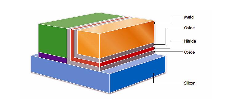
Fig 2: Renesas' SG-MONOS flash memory design is said to withstand 250,000 program/erase cycles
But it says employing a fin structure for embedded flash memory can present a big challenge, depending on the structure of the flash memory. Two types of embedded flash memories have been proposed and implemented – floating-gate and charge trap.
Renesas says the charge trap approach, which it has used recently, can retain charge better and has shown more reliability in applications such as automotive MCUs. It adds that, since the functional material of the memory is formed on the surface of the silicon substrate, it is ‘comparatively easy’ to extend the design into a 3D fin structure. In contrast, it notes, the complex structure of floating-gate flash memory cells makes it difficult to integrate them into a fin structure.
Renesas also points to another advantage of SG-MONOS compared to the floating gate approach – the memory cell structure is maintained after the dummy polysilicon gate electrode used in the manufacturing process is replaced with the metal gate electrode.
With a fin structure, field enhancements at the tip of the fins may affect device performance. This can be overcome using a ‘step pulse’ programming method in which the programming voltage is raised stepwise. This is said to have reduced degradation over time in fin-structure SG-MONOS memory cells and Renesas believes the technology will support 250,000 program/erase cycles.
Renesas concludes that fin-structure SG-MONOS memory cells have ‘promising characteristics’ and are likely to support random access reads at frequencies in excess of 200MHz.
imec develops STT-MRAM for 10nm processes The imec team says significant challenges remain before the technology can be commercialised, including scaling for higher densities and increasing the device switching current. Its p-MTJ stack features a free layer and a reference layer comprising CoFeB based multilayer stacks. Developed on 300mm silicon wafers, the memory is said to be compatible with CMOS back-end-of-line technology. Gouri Sankar Kar, who coordinates imec’s STT-MRAM activities, said: “Our demonstration of a high-performance p-MTJ device as small as 8nm, combined with a manufacturable solution for a scalable STT-MRAM array, will open up continued innovations for embedded non-volatile memory applications at the 10nm node.” |


