
While there has been a lot of hope and hype around printed electronics, the market is finally catching up to the technology. The printed and flexible electronics market is expected to hit more than $73billion by 2027, according to IDTechEx.
Much of this market includes organic light emitting diodes and conductive ink that’s used in a broad range of applications. It’s also being driven by the Internet of Things, which demands low-cost, lightweight technologies.
At their core, designs for traditional PCBs and printed electronics deliver very much the same thing - connected electronic components form an electronic circuit that powers a product.
However, how printed electronics are built and what materials they are built with are very different.
In traditional PCB design, an electronics engineer designs the board, defines its dimensions based on electrical and some mechanical requirements and when ready releases the manufacturing files. The manufacturer then manufactures the PCB according to design files by etching away copper or other conductive materials to form a trace with the right dimensions that full-fill electrical requirements.
The process involves multiple layers and the use of a lot of hard, laminated materials.
In printed electronics, the same results need to be achieved, but with the use of different design rules, materials and manufacturing methods. While traditional PCB design and the manufacturing or printing process typically involves reducing materials (etching) to form a trace, printed electronics is an additive process.
Materials are added onto existing surfaces not with layers but by printing directly onto a substrate. For example, if a signal pathway needs to cross an existing pathway, a designer can print a small patch of insulation directly in the required location to enable the new signal pathway to be printed across the existing pathway without causing a short.
Typically, printed electronics are easier to produce, lighter than traditional circuit boards, cheaper to print, quicker to assemble, and offer more design freedom.
Today, printed electronics have the potential to disrupt conventional technologies, overcome limitations in components or the manufacturing process and even create new markets.
The potential applications are diverse: medical diagnostic devices, smart packaging, clothing, batteries, sensors, drug delivery devices, flexible solar cells, displays, lighting products, injection-moulded electronics and more. Think wearables, glucose test strips and self-darkening windows to name but a few.
Injection moulded electronics
Injection-moulded electronics (IME), for example, are a new way to design and manufacture products in industries spanning automotive, appliances, IoT and industrial markets. With 3D technology, developers can simplify multi-part, complex electronics and replace them with durable, lightweight single-piece structural alternatives that integrate sensors, controls and other elements to produce smart electronics for today’s consumers. IME integrates a number of broadly applied production technologies - flexible circuit printing, printed electronics, surface mounting of electronic components, in-mould labelling thermoforming and injection moulding - into one method that enables the mass production of 3D structural electronics with specific benefits in automotive.
But printed electronics come with their own unique challenges that need to be addressed at the design stage. Printed electronics are typically designed in 2D for a flat board, but once sent for printing and manufacturing, the electronics will be made to fit unconventional shapes and spaces. Routes and traces designed in a 2D environment won’t always work as intended once they’re bent and stretched to fit the angles and shapes when they’re printed.
Essentially, designers need to break free from the traditional layers and organisational constructs seen in traditional PCB designs; design in a fluid space rather than horizontal and vertical design in 2D and visualize in 3D. They need to be able to route and design in 3D, but not in layers. Apart from the substrate that the design is printed on, there are no physical layers in a printed electronics product - conductive pathways are printed directly onto the substrate.
There are also considerations of integrating ECAD and MCAD requirements as you move into a fluid 3D environment. Will the circuit you designed in 2D fit the 3D mould?
Additionally, consideration is key between the compatibility of the conductive material and the surface that it will be used on; flexibility, adhesion measured by the material’s ability to stay on the product surface, and durability to heat and strain. The most important questions arise asking how the product will be used.
Simulations must test usage as in real world conditions:
- How people will move with the item?
- How often will it be used?
- When will it be used?
- The environment in which it will be used?
- Will it interact with other more complex systems or is it standalone?
The same physical laws govern the design of PCB and printed electronics, and essentially define what’s possible to design. Although two circuits - one made for a PCB and another for printed electronics - can have exactly the same functionality, but the circuit implementations are quite different. This is because of the physical capabilities and limitations of the material used in electrical circuits. In both circuits, voltage differences must be applied over impedance of the routes made of difference conductive material. To get the same current flowing in both circuits requires adjusting impedances to the same level or setting circuit-specific voltage levels. This typically involves a good bit of trial and error with impedances and voltage levels.
Choosing the right materials can be a challenge in printed electronics design. Extreme heat is required in the thermoelectric and molding process. The same goes for the thermoplastic simulation process.
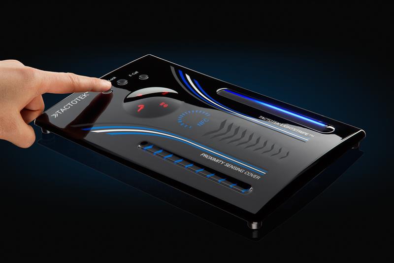
Above: Finnish company Tactotek encapsulates flexible film electronics within injection moulded plastics, which creates smart surfaces
A lot of progress has been made with materials, particularly in the area of conductive and dielectric inks designed to withstand extreme heat. Conductive inks such as silver, carbon and other polymer thick films (PTF) can be printed on various substrates that on their own are lighter than those used in traditional PCB design. These include polyester, polycarbonates, polyurethanes, and paper and hold the potential for enabling more creativity and less complexity in product development.
Designers now have access to a wide material library section of not just different types of inks but adhesives and materials, including ink, that are stretchable. The ability to access and correctly select the right materials are crucial to printed electronics design.
As printed electronics become more mainstream across all industries, PCB designers must evolve their skills and experiences to encompass new technologies. In the near-term, printed electronics will likely continue to be used in combination with PCBs, but eventually printed electronics will displace many rigid and rigid-flex PCB designs as more products rely exclusively on printed electronics. That’s because printed electronics will allow products to be more perfectly customised.
Industry also needs to coalesce around standards, such as the standardisation of file exports, and more manufacturers must ensure they have the materials for printed electronics. While we don’t yet have the rules or best practices for how to design for printed electronics, like 3D, printed electronics are here to stay.
Author details: David Haboud is a Product Marketing Engineer at Altium


