
Fortunately, advances in 3D printing and additive manufacturing promise sweeping change, resulting in new developments in electronics products that will help to make them smaller, faster, lighter, lower power and more feature rich.
Every electronic device is built around a PCB. Until now, creating prototypes of PCBs has been a time-consuming process. But new technology now exists that allows companies to take full control of their development cycles by 3D printing prototype circuits in-house. Leveraging additive manufacturing for PCB prototypes helps to reduce design and test cycles from months or weeks to days or even hours.
In-house prototyping opens up a whole new world for design engineers, who can now streamline and control the entire process – from proof of concept, to design validation, to producing high resolution multilayer PCB prototypes. Development teams can introduce more agile development workflows to reduce time-to-market and increase innovation.
As an example, current workflows generally lead to infrequent and relatively large prototype batches. Imagine being able to print and test 10 different designs over a week, rather than getting a batch of one design, as is the case today.
Other benefits of 3D printing prototypes in-house include:
• Rapid innovation gives design teams the freedom to experiment and think ‘outside the box’.
• 3D printers can print complex geometries with structural and functional characteristics to save space, weight and cost.
• The capability enables greater flexibility and customisation in PCB design and, ultimately, the potential for small-scale production.
In-house prototyping
A survey conducted amongst PCB designers and manufacturers, electrical engineers, OEMS and others interested in 3D-printed PCBs and circuits revealed that most companies are employing external services to create PCB prototypes. It also showed they are investing large amounts of money and significant time into their production.
According to the survey, there is also increasing demand for in-house prototyping for research and product development. This is not surprising, since businesses need to quickly respond to changing customer and market demands in this highly competitive industry.
The applications for 3D printed electronics are endless for any product in the consumer electronics, medical devices, defence, aerospace, automotive, IoT and telecom sectors, where miniaturised design and weight are major factors. These sectors are poised to benefit significantly from flexible, rigid-flex and multilayer 3D printed PCBs for rapid prototyping and short-run manufacturing.
Additive manufacturing comes of age
Additive manufacturing describes the process of creating 3D objects by depositing material layer by layer. One of the world’s largest manufacturers – General Electric – intends to use additive manufacturing to produce a fuel nozzle for a new aircraft engine by printing the part with lasers, rather than casting and welding metal. The technique could transform how GE designs and makes complex parts for a range of products.
GE and other well-known manufacturers are turning to additive manufacturing because it saves time, enables high-precision production, uses less material and produces less waste than conventional processes, and as a result, saves money. As a result, long tail products, customisation and non-planar circuits can be added to the consideration set.
Similarly, digital fabrication for printed electronics uses high resolution inkjet printers, which deposit functional inks layer by layer. These specialised printers work with sophisticated proprietary software that helps manage the printing process.
Using additive manufacturing for electronics gives designers options for replacing existing subtractive manufacturing of PCB prototypes, which is an expensive, time-consuming, polluting, multi-stage, labour and material intensive process.
Using in-house 3D printers, designers can create multilayer electronics in a matter of hours. The process even enables the printing of complex elements – such as vias in pads, blind or buried vias and through-holes – without the need for etching, drilling, plating or generating waste. The dielectric serves as a solid support within which the conductive drops are deposited, layer by layer, at the precise XYZ coordinates specified to create the traces and interconnects. The printer will produce a fully-functional multilayer circuit in one overnight print job. Upon completion, the multilayer 3D printed PCB is ready for soldering.
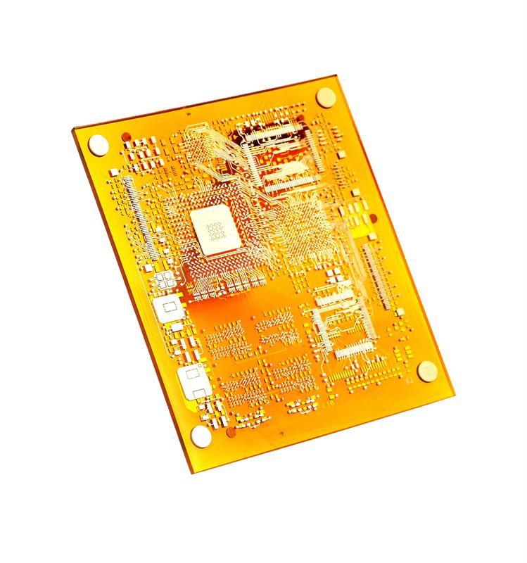 A multi-layer 3D printed board created using the Dragonfly 2020 printer
Easy as 1, 2, 3
As complex as it all sounds, advanced additive manufacturing technology makes it possible to print a PCB prototype with the simplicity of pushing of a button. This capability empowers designers to iterate on the fly, to catch and correct errors quickly and to take risks that might otherwise be too costly and time consuming if prototyping is done offsite.
While this process is simple for the end-user, the technology that makes it possible is highly complex. The team at Nano Dimension has spent years developing the tools and technologies necessary to make 3D-printed PCBs and circuits a reality: an extremely precise inkjet deposition printer, customised conductive and dielectric inks that can be 3D printed simultaneously, and software capable of converting complex schematics into print instructions.
The DragonFly 2020 3D printer is the first device in the industry that enables electronics companies to create their own professional, high resolution multilayer PCBs and 3D circuitry for rapid prototyping and small-scale production – printing a PCB layer by layer.
For designers, the process is as straightforward as loading the design file straight to the 3D printer and then printing. The Nano Dimension Switch software (job editor) accepts common file formats in the electronics industry – Gerber and Excellon – streamlining prototype fabrication significantly. Multilayer 3D files can be edited and prepared from standard files, and the software allows for adjustments to numerous parameters such as layer thickness. Starting from a sacrificial substrate, the materials are built up from the underside conductive traces and solder mask, to finish with the topside pads and solder mask.
With today’s advanced printing capabilities, designers and engineers are able to develop different sections of the circuit in parallel – testing and iterating on the fly to accelerate creativity and improve quality. The result is reduced development time, improved innovation and fewer development risks and rework. This enables companies to bring better electronics to market faster without exceeding budget, while keeping sensitive design information in-house.
Author profile: Robert Even is materials manager at Nano Dimension.


