
While 3D printing is being used for a variety of professional and hobbyist applications, it is only recently that we have seen developments in this technology for electronics such as PCBs.
At each stage of product development, electronics designers and engineers have to get prototype boards in hand for testing purposes. The current standard subtractive manufacturing of PCBs is a multi-stage process that is labour and material intensive and is often outsourced.
Over the course of design and testing, the time spent waiting for complex prototypes can add up to weeks, hardly rapid prototyping. Moreover, if the prototype reveals any flaws, it takes additional days or weeks to redesign, then get the fixes tested before the design can go into production, presenting a business risk to on-time product development.
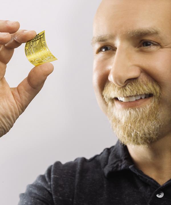
Last year, Nano Dimension introduced a 3D printing system specifically designed for printing professional PCB prototypes in-house. The DragonFly 2020 3D Printer brings together an extremely precise inkjet deposition 3D printer, advanced nano chemistry and sophisticated software capable of meeting the needs of rapid prototyping and can significantly reduce the time spent on prototyping from weeks to hours – even for the most complex PCBs. This allows designers to build and test partial boards, or change designs on the fly. The result is that new prototypes can be built and tested on the same day.
The printer can also save money and even allow users to create models that would normally be difficult or even impossible to produce, or that would be time intensive using current manufacturing processes. Ultimately, this could increase the quality of the final product and even produce a whole new world of electronics.
The printer is able to offer high resolution, conductivity and speed. Quick prototype turnaround times and more frequent iterations mean PCB designers will have more freedom to express what they imagine, can experiment with different geometries and designs, leading to fewer errors and better products.
In the long run, the time savings can translate into increased efficiency, shorter lead times and cost savings.
In addition, incorporating additive manufacturing into PCB fabrication means that no raw material goes to waste, unlike when copper is etched or holes drilled by conventional methods.
Multilayer PCBs
At the basic level, it is a three axis inkjet printer that deposits layer upon layer of conductive and dielectric nano-particle inks. The process is repeated until a 3D multilayer PCB is built up. Each pass of the print head deposits a 2µm layer of material (dielectric or conductive) at the exact location specified by a Gerber design file. This is enabled by software developed in-house that converts Gerber files into 3D printable files, from which the printer builds up the PCB.
For more complex PCBs, vias in corresponding positions on different layers, can be added to this process, enabling the creation of electronically connected blind, open or complete vias. Through-holes are also created building surround materials around a void and creating geometries that would be impossible using traditional techniques. More importantly, the technology can produce denser circuitry on a smaller object and, because the PCB no longer needs to be rectangular, it is possible to embed circuitry into 3D created cavities.
| Designers will be able to go beyond traditional PCB designs with new 3D printing systems. (Pic: Yoram Reshef) |
It is in the development of denser circuitry that 3D printing is able to offer a broad range of new possibilities as the materials and software offerings mature.
Leaving the world of planar circuits and moving into 3D circuitry allows for the beginnings of printing embedded passives, particularly resistors. As the 3D printing starts to integrate pick-and-place capability, the prospect of placing, embedding and then overprinting components becomes a reality.
All this brings together the possibility that in time PCBs, as we know them, will become obsolete and structural objects will come to contain the required circuitry and sensors within them. Imagine the advantages in terms of weight savings, miniaturisation, reliability and overall end-product practicality in a world where structural objects or subsystems include electrical functionality.
When it comes to the result of a print job it is essentially a solid dielectric piece inlaid with silver conductive traces at the precise XYZ coordinates specified by the Gerber file.
To achieve the highly conductive fine traces, Nano Dimension has developed proprietary AgCite silver nanoparticle inks and high-performance dielectric inks for inkjet deposition. These two materials are critical because they must provide just the correct amount of adhesion to work with a variety of substrates. The inks deliver properties including conductance, controlled impedance, and other specific mechanical properties enabling multilayer boards and various electronic applications such as RFID tags and sensors.
A patented, highly efficient and environmentally responsible nanoparticle synthesis process enables the unique properties of AgCite inks. Developed by the Centre for Nanotechnology at the Hebrew University of Jerusalem, the synthesis process, which begins with a silver precursor raw material, allows for a much finer control of the size, shape and distribution of the silver nanoparticles in accordance with customer’s printing requirements. The synthesis process is critical to the types of nanoparticles and ink formulations that can be produced.
Nano Dimension is now looking to expand the scope of 3D printing, with the development of highly conductive copper-based inks that may, one day, replace more expensive silver inks.
Copper’s low price gives it a significant advantage in the market when compared to silver ink, which is generally limited to prototyping applications.owever, since the copper nanoparticles rapidly oxidize upon contact with air, this impairs the electrical conductivity and ability to print copper with 3D digital printers.
To solve this problem, Nano Dimension has filed a patent for a new approach to copper nanoparticle development. The company plans to continue expanding the range of materials it can print onto and into circuits. A recent collaboration with Tel Aviv University on the development of nanoparticle nickel ink is an example of how Nano Dimension is seeking to deploy the mechanical strength and ruggedness of nickel to overcoat coppers or build 3D printed sensors.
3D printing has made significant advances in recent years, with much diversification in the types of materials and printers available. As designers embrace and discover new applications for 3D printed electronics, it is only a matter of time before we will start to see innovative PCB designs that are not constrained to flat layers on a rectangular board or limited to prototyping.
| Author profile: Simon Fried is chief business officer and co-founder of Nano Dimension. |
 |


