
The problem for any configurable device like an FPGA is its hunger for routing resource – it needs far more than an ASIC built using dedicated masks. This tends to spread logic blocks further apart to avoid routing congestion. But performance calls for closely related logic circuits to sit near each other.
“Most of the delay is in the routing,” says Craig Davis, senior project marketing manager at Intel’s programmable systems group. This consideration makes the interaction between placement and routing one of the most important factors in high-performance design. Complex logic blocks and hardwired cores that are fixed in place constrain the job of the placement and routing and can easily lead to unwanted congestion. The tools used today place a strong emphasis on alleviating this congestion and in reducing the impact of routing delays.
Specialised resources within FPGAs often provide mechanisms for freeing up routing and so avoid the congestion that can lead to designs that run slower than expected. Xilinx tools will, for example, move signals with very high fanouts onto global clock trees if they are not required for clock distribution in the design. Ron Plyler, Xilinx’ product marketing manager for physical implementation tools says the optimisation techniques were conservative for the Virtex 7 series but can be more aggressive on the more recent UltraScale families because they “have a much richer and more flexible clocking architecture, which enables a superset of 7-series optimisations”. He adds: “This happens at the end of placement when the global clock placement and resource allocation is settled and timing estimates are more accurate.”
Plyler says a common technique for reducing congestion overall is to focus on the Rent exponent – a measure of the number of connections each block within the design needs. Tool reports provide connectivity measurements for each block and the optimisation tools can focus effort on elements that tend to increase the Rent exponent. “These strategies reduce congestion by selectively reducing the utilisation of structures that tend to increase Rent and congestion,” Plyler says. Those structures include slice multiplexers, carry chains and LUTs with more than one output.
“Another area where we are focusing effort on reducing congestion is to provide specific recommendations,” Plyler says. These are through a report that offers quality-of-results suggestions. “These are more on the level of ’surgical strikes’ where we try to pinpoint exact causes of congestion and identify specific logic to refine. We also plan to integrate our incremental compile flow to both increase predictability and reduce the overall compile time it takes to incorporate suggestions and evaluate their successes.”
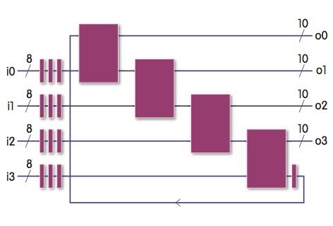
| Below: Motivating example – four slow combinational blocks and a tight feedback loop that cannot be timed |
In its Stratix 10 family of devices, Intel’s programmable systems group decided to place registers at every possible switching location within the programmable interconnect to support a number of common timing-improvement strategies. The ‘hyper-registers’ have limitations – they do not have asynchronous-reset inputs so as not to consume excessive routing resource – but their sheer number is intended to create many more opportunities for pipelining.
“It’s a mux and a register, and it’s bypassable. With a configuration bit you can choose which registers to use late on in the design flow.” Davis says.
Traditionally, adding pipeline stages involves routing to a register that sits alongside a LUT, all of which incurs a delay. Ideally, the tools would pick up a LUT halfway along the original path to balance the delay. As device utilisation increases, this becomes difficult. “With hyper-registers, you’ve got so many you can generally put the new register smack in the middle every time,” Davis claims.
Some circuits do not benefit from pipelining because they employ long feedback paths. Intel recommends the use of Shannon decomposition, which demands more intensive changes to the RTL. When the optimisation work it can push the feedback loop down to a single multiplexer by reconfiguring the logic that feeds into that final logic stage. In effect, the logic precomputes values ready for the final decision taken by the gate with the feedback element.
Intel’s Quartus tools help identify opportunities for pipelining and more advanced transformations such as Shannon decomposition. “It will do speculative changes to your design: what happens if I take asynchronous clears out of the design? That often provides more opportunities for retiming so it can show the increase in clock speed if I put the registers in,” Davis says.
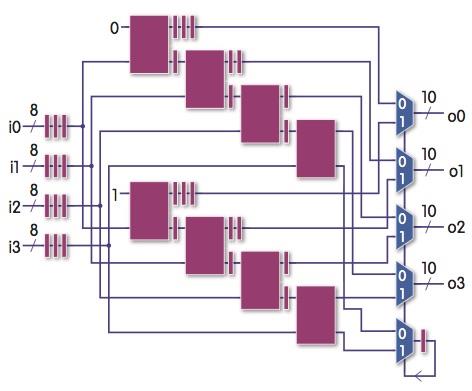
| Below: Retiming has reduced cycle time to one block's delay plus a multiplexer |
Even without RTL changes, there are many complex combinations of settings the design tools understand that provide opportunities for optimisation. Singapore-based EDA tools supplier Plunify has found machine learning to be an effective way to unlock effective combinations for different types of FPGA design.
Plunify’s algorithms have found cases where moving logic out of hardwired blocks can improve overall timing, possibly because it can reduce the congestion caused by the need to dedicate routing to connect to the fixed-location cores. “Sometimes we are surprised by the algorithm. Even though, from a hardware designer’s point of view, one should utilise as many DSPs as possible, a group of settings that limit the number of DSPs that you use in a design can result in drastic improvements,” says HarnHua Ng, co-founder and CEO of Plunify.
The key to determining the effective combinations involves many compilation runs. Plunify originally launched its InTime optimiser last year for use by customers on their own design databases. “Because it’s machine-learning software, more data is required than the average FPGA flow generates,” Ng explains, noting that customers may not have sufficient servers to support the data-gathering process. Earlier this year, Plunify introduced a service to do the analysis based on its accumulated data and make the configuration changes that will improve timing.
| "Another area where we are focusing effort on reducing congestion is to provide specific recommendations through a report that offers quality-of-results suggestions." Ron Plyer, Xilinx’ product marketing manager for physical implementation tools |
Plunify co-founder and COO Kirvy Teo adds: “In terms of what can be done, we have seen designs pass timing from as bad as 2ns worst negative slack. The results have surprised even ourselves. Usually what happens is that, when we get a design, the user has tried all the aggressive settings that they can get their hands on. Usually it doesn't get the best results. But we have found groups of settings that work better. If you set everything to be aggressive the software churns without getting good results.
“For this to work you need a lot of data. Each time you run you should store data and use that for your next runs and that will really change the game. The one with the most data will win this ultimately. The difficult part is how to use this data but that has always been a challenge for machine learning apps,” says Teo.
The rise of machine learning and the response from FPGA makers will see a further level of complexity added to the design process. Victor Peng, Xilinx CEO sees “an explosion of data” coming: “It will require a different form of computing. We are really at an inflexion point where we have moved beyond the FPGA. It is a new product category: the heterogeneous processing platform. Because of that, we will be able to accelerate a broad range of workloads.”
In the case of Xilinx’s upcoming Project Everest devices, a network-on-chip will help reduce congestion across the devices, which will deploy billions of transistors through the use of a 7nm process. The NoC is intended channel data between the programmable fabric and specialised compute engines designed for tasks such as machine learning, alleviating congestion in the finer-grained routing fabric. It will represent one more step in the war against congestion in programmable devices.


