
Advances in semiconductor technology have enabled the proliferation of phased array antenna with active electronically scanned antenna (AESA) advancing in satcom on-the-move and 5G communications.
Electrically steered phased array antennas offer benefits such as having a lower profile, less volume, improved long-term reliability, faster steering and multiple beams.
A key aspect of the phased array antenna design is the spacing of the antenna element and the half-wavelength element spacing needed for most arrays does create particularly challenging designs at higher frequencies. Consequently, ICs at higher frequencies are now more integrated and packaging solutions have become more advanced.
Semiconductor technology is looking at more advanced silicon ICs that combine digital controls, memory, and RF transistors onto the same IC. Gallium nitride (GaN) is also significantly increasing the power density of power amplifiers to offer a smaller footprint.
Phased array technology
There is a major push toward low profile arrays with less volume and weight. Designs are moving from a ‘plank’ architecture to a flat-panel approach, reducing the depth of antennas and making them easier to fit.
In planar array designs, the space available for ICs on the back side of the antenna is limited by the antenna element spacing – e.g. the maximum antenna element spacing to prevent grating lobes for up to a 60° scan angle is 0.54 λ. As you go higher in frequency, the spacing between the elements becomes quite small, leaving little room for components behind the antenna.
More integrated ICs help to reduce the challenges in laying out the antenna design with the required spacing. With more electronics packed into a reduced footprint, antenna’s demand new semiconductor and packaging technology to make solutions viable.
The microwave and mmWave IC components used as building blocks for a phased array antenna are shown in Figure 1.
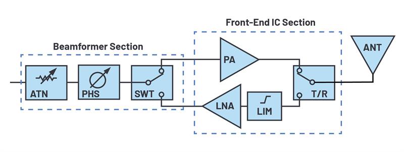
In the beamforming section, the attenuator adjusts the power level at each antenna element so that the sidelobes of the antenna pattern can be reduced. The phase shifter adjusts the phase of each antenna element to steer the antenna’s main beam, and a switch is used to toggle between transmitter and receiver paths.
In the front-end IC section, a power amplifier is used for the transmit signal, a low noise amplifier for the received signal and another switch is used to toggle between the transmitter and receiver. In past implementations, each of these ICs was offered as separate packaged devices.
More advanced solutions could have an integrated monolithic single-channel gallium arsenide (GaAs) IC to achieve this functionality. Included in most arrays before the beamformer are a passive RF combiner network, receiver/exciter and signal processor.
The recent proliferation of phased array antenna technology has been aided by advancements in semiconductor technology. The advanced nodes in SiGe BiCMOS, silicon-on-insulator (SOI), and bulk CMOS have combined digital and RF circuitry and can perform the digital tasks in the array, as well as control the RF signal path, to achieve the desired phase and amplitude adjustment.
It’s possible to achieve multichannel beamforming ICs that perform gain and phase adjustment in a 4-channel configuration, as well as up to 32 channels aimed at mmWave designs.
In some lower power examples, a silicon-based IC could be a monolithic solution for all the previous functions. In high power applications, gallium nitride-based power amplifiers significantly increase the power density that may be fitted into the unit cell of a phased array antenna.
In airborne applications, there’s a trend to flat-panel architectures with the power added efficiency (PAE) benefits of GaN technology. GaN has also enabled large ground-based radars to move from a dish antenna, driven by a TWT, to phased array-based antenna technology, driven by solid-state GaN ICs.
Monolithic GaN ICs are capable of delivering over 100 W of power with over 50% PAE. Combining this level of efficiency with the low duty cycle of radar applications allows for surface-mount solutions where it is possible to dissipate the heat generated through the package base.
High reliability designs may use gold plated, hermetically sealed housing with chip-and-wire interconnects inside and are more robust for extreme environments, but are larger and more costly.
Multichip modules (MCMs) combine numerous MMIC devices, as well as passives, into a relatively low cost surface-mount package. MCMs still allow for the mixing of semiconductor technologies so that the performance of each device can be maximized while saving considerable space.
Phased array beamformer ICs
Integrated analogue beamforming ICs - core chips - are being developed to support a range of applications including radar, satellite communications and 5G telecommunications. The primary function of these chips is to accurately set the relative gain and phase of each channel so that signals add coherently in the desired direction of the antenna main beam.
They are being developed for analogue phased array applications or hybrid array architectures that combine some digital beamforming with analogue beamforming.
An example, is the ADAR1000 X-/Ku-band beamforming IC which is a 4-channel device covering 8 GHz to 16 GHz operating in time division duplex (TDD) mode with the transmitter and receiver integrated into one IC.
In receive mode, input signals pass through four receive channels and are combined in a common RF_IO pin. In transmit mode, the RF_IO input signal is split and passes through the four transmit channels.
A simple 4-wire serial port interface (SPI) controls the on-chip registers, while two address pins allow SPI control of up to four devices on the same serial lines. Dedicated transmit and receive pins provide synchronization of all core chips in the same array. A single pin controls fast switching between the transmit and receive modes.
The 4-channel IC is housed in a 7mm × 7mm QFN surface-mount package for easy integration into flat-panel arrays and addresses some of the size, weight and power challenges in high channel count phased array architectures.
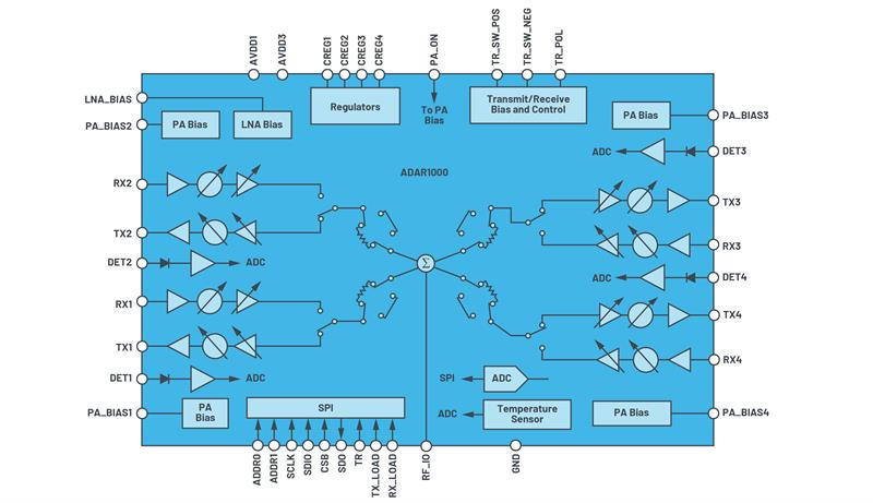
The device dissipates only 240 mW/channel in transmit mode and 160 mW/channel in receive mode per channel.
The transmit and receive channels are brought directly external and designed to mate with a front-end IC. A full 360° phase coverage with phase steps less than 2.8° and over 30 dB of gain adjustment can be achieved.
The ADAR1000 contains on-chip memory to store up to 121 beam states with each state containing all phase and gain settings for the entire IC. The transmitter delivers approximately 19dB gain with 15dBm of saturated power, where the receive gain is approximately 14dB. Another key metric is the phase change over gain setting, which is approximately 3° over a 20 dB range. Similarly, the gain change with phase is about 0.25 dB over the entire 360° phase coverage, which eases the calibration challenges.
Complementing the ADAR1000 beamforming chip is the front-end IC, the ADTR1107.
The ADTR1107 is a compact, 6 GHz to 18 GHz, front-end IC with an integrated power amplifier, low noise amplifier (LNA), and a reflective single-pole, double-throw (SPDT) switch.
This IC offers 25dBm of saturated output power (PSAT) and 22dB small signal gain in the transmit state, and 18 dB small signal gain and 2.5dB noise figure (including the T/R switch) in the receive state. The device has a directional coupler for power detection. The input/outputs (I/Os) are internally matched to 50 Ω. The ADTR1107 is supplied in a 5 mm × 5 mm, 24-lead, land grid array (LGA) package.
The ADTR1107 has been designed for easy integration with the ADAR1000.
Highly integrated radio frequency transceiver chips contribute to more integration at the antenna level.
The ADRV9009 is an example of such a chip. It offers dual transmitter and receiver, integrated synthesizer, and digital signal processing functions.
The device includes a state-of-the-art direct conversion receiver with high dynamic range, wide bandwidth, error correction, and digital filtering built in. Auxiliary functions include an analogue-to-digital converter (ADC) and a DAC.
General-purpose inputs/outputs for the power amplifier and RF front-end control are also integrated. A high performance phase-locked loop provides fractional-N RF frequency synthesis for the transmitter and receiver signal paths. It also offers low power consumption and comprehensive power-down modes to further conserve power when not in use. The ADRV9009 is packaged in a 12mm × 12mm, 196-ball chip scale ball-grid array.
The advances in IC design described here have resulted in a technology shift in antenna designs and are helping to fuel changes across multiple industries.
Author details: Jeff Lane is a Product Marketing Engineer, Analog Devices


