
They are popular due to their compact size, which makes them suitable for small devices. However, as connected devices become smaller and continue to shrink, designers need to squeeze their chosen antenna solution into even smaller PCBs.
SMD antennas may be the obvious choice for a small PCB, but there is an alternative. Flexible printed circuit (FPC) antennas can be a better fit in certain designs. FPC antennas are widely used in applications where there is insufficient space for a SMD antenna.
As devices shrink and space for the components becomes more limited, the board layout requires more care.
SMD antennas offer the advantage of fitting into small spaces on the PCB. Flexible antennas are used differently. They are extremely slim, typically just 0.15mm thick, which means they can be used in slim, lightweight devices, or they can be folded and tucked into the housing of the device.
Ground plane
With an SMD antenna, the design needs to allow for a ground plane, but FPCs do not require one.
So why does the SMD require a ground plane? Other forms of dipole antennas use two radiators which work together, where the length of each radiator is related to the wavelength of the frequency. SMD antennas have only one radiator, so in their case, the host PCB, which is also a conductive surface, becomes the second radiator through reciprocity. This means that the ground plane length is important. It must relate to the lowest wavelength, but if it is too short the antenna will lose efficiency. SMD antennas are designed to be used in different positions on the PCB, and each has its own individual ground plane requirements. For example, some are designed to be placed on an edge of a PCB, and some are designed for a corner. A PCB designer should choose the antenna that suits the design best, and also allow for the ground plane, which will be specified in the manufacturer’s datasheet.
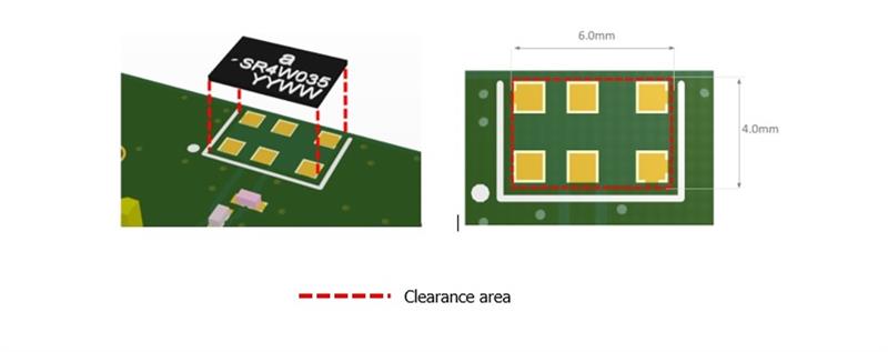 Above: This particular SMD antenna is used in the centre of the longest edge of the PCB and the ground plane, or clear out area, is the same size as the antenna
FPCs do not require a ground plane to radiate, which means they allow the designer more freedom to arrange the components in the circuit within the design.
Connection to other components
Both SMD and FPC antennas need to be designed-in with care. The FPC is different to the chip antenna in that the coax cable actually becomes an active part of the antenna when it is working. This means that the routing of the cable is very sensitive, and there is a risk that the antenna could pick up noise from other components close by. We advise routing the cable with care, to avoid interference from any other component. A DC blocking capacitor should be placed in line to protect the RF front end.
The same integration rules apply for SMD and FPC antennas. All transmission lines should be designed to have a characteristic impedance of 50Ω.
At Antenova, we recommend that the transmission lines should be kept as short as possible, and that any other parts of the RF system like transceivers, power amplifiers, etc., should also be designed to have an impedance of 50 Ω.
The thickness of the PCB and the dielectric constant of its material is important. When the material for the PCB has been chosen, a coplanar transmission line can easily be designed using one of commercial software packages for transmission line design. These calculate the appropriate transmission line width and the correct gaps to ground to allow on either side of the feed for the thickness of the PCB, copper and substrate. FPC antennas are supplied with I-PEX MHF (U.FL) type connectors to connect them to the host PCB or wireless module, which often has the mating I-PEX MHF connector to join directly, with the cable in varying lengths. This gives the designer further options for positioning the antenna within the device.
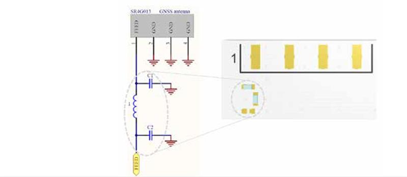
Above: Pi Matching Network example
Matching
An SMD antenna requires matching to the other RF components in the design to optimise its performance for the bands of interest in situ. Antenna matching is the process of aligning the impedance of the antenna chip with the other RF circuitry in the design, and it increases the performance of the antenna by optimising the impedance for the bands of interest.
Trace lines (or transmission lines) carry the RF signals to and from the antenna and the characteristics of these lines typically yield low levels of resistance when designed properly. The power transfer and return loss of an antenna can be as high as 50% in a poorly matched design. Trace lines operate at 50Ω, so RF traces and other elements of the RF system - such as transceivers or power amplifiers—must therefore match this impedance.
I would suggest the use of grounded coplanar waveguides (GCPW) for embedded antennas, as the antenna can be mounted on the component side of a PCB and achieve better performance levels. They also remove the need for backside manufacturing processes for the PCB. The quality of the impedance match is measured as the VSWR (Voltage Standing Wave Ratio) or Return Loss. This is one of the most critical parameters in antenna integration, as a well-matched circuit can provide good levels of performance, even when its efficiency is inhibited. Using Pi matching circuits between the antenna terminal and the 50 Ω input ports to optimise the power transfer in the bands of interest, is recommended.
If the device is likely to be used in the hand or close to the human body as in the case of trackers and wearables devices, the antenna should be matched and tuned according to the operational environment. With the FPC antenna, very little tuning or matching is required. The production process may affect your choice of antenna. Chip antennas are compatible with the pick and place machines, while flexible antennas are fixed in place by a peel-back adhesive strip on one side. FPCs are a good solution for smaller production runs and often require hand assembly.
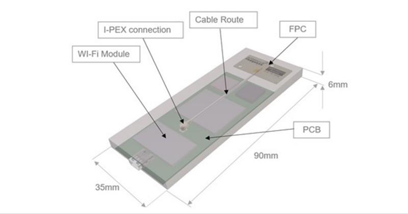
A slim design with the FPC integrated inside and cable route
Summary
In the end the final choice of antenna will depend on the shape of the device, the space available on the PCB, and the eventual manufacturing process.
Chip antennas function very well in small devices provided there is enough space for them to perform correctly and they are very popular. They require space for a ground plane, as specified by the manufacturer, and need to be placed away from components that create “noise”. If the space on the PCB is limited the FPC may be the way forward. The FPC option is also good for devices with a longer chassis. FPCs, being larger, will probably not be your first choice for smaller devices, but they can work well for projects that suit them. Folding the antenna and inserting it inside the casing of the design helps to keep it away from other, potentially interfering, components.
Author details: Geoff Schulteis is Senior Antenna Applications Specialist with Antenova


