
The arrival of dark silicon has taken longer than originally expected, but the problem is getting more pressing as chip designers exhaust their ability to squeeze more efficiency from traditional architectures. Increasingly, the focus is falling on how processors interact with memory.
Research by James Balfour at Stanford University in the late 2000s found it takes three times as much energy to write the result of a 32bit addition to a nearby register than it does to perform the calculation. Push that data into a cache and the energy cost increases 25 times, due largely to the capacitive charging needed to access memory arrays.
What if you could put logic and memory together in the same circuit and make digital logic stateful? At some point, large amounts of data will need to be written out to long-term storage. While computers based on integrated logic and memory would still incur those costs, tighter integration of logic and memory could greatly improve energy efficiency.
One answer to stateful circuitry comes from exploiting magnetism at the quantum level. Two decades ago, Slonczeswki at IBM and Berger from the University of Pittsburgh predicted independently an effect they expected to find in read-write heads of hard disk drives and other devices that exploit giant magnetoresistance.
The core structure they proposed is a non-magnetic layer sandwiched between two magnetic layers. One magnetic layer has a fixed magnetic direction; the other can move freely. When a current passes through the stack from the direction of the fixed layer, the electrons become spin-polarised due to the magnetic field.
If the magnetic fields are not aligned, as carriers pass through the free layer they start to align with the spin of that layer. The reduction in the spin component orthogonal to that of the free layer, through conservation of angular momentum, produces a torque on the layer (see fig 1). This torque can shift the magnetic orientation of the free layer itself. In this way, a magnetic state can be written to it by passing a large enough current through.
Different current profiles can produce oscillations, useful for generating and detecting microwaves, and flip the orientation in the opposite direction. Changes in relative magnetic orientation between the layers restricts current flow to varying degrees, leading to the main use so far for the spin-torque transfer (STT) device as a memory. Everspin started shipping a 256Mbyte magnetic memory (MRAM) based on STT in the summer.
One modification is to have opposite magnetic orientations on either side of a domain wall in the free layer. Torque transfer in this case can shift the position of a domain wall and the device becomes a form of memristor, where the stored resistance of the device is a function of the charge (see fig 2). The memristor is a behaviour predicted in 1971 by Professor Leon Chua on the basis that symmetry predicted a fourth basic type of passive device alongside resistors, capacitors and inductors, but which appeared to be missing in nature.
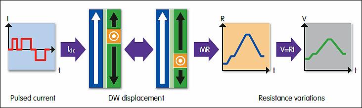
Figure 2: Torque transfer can shift the position of a domain wall, allowing a memristor style device to be created
Since the first reliable discovery of memristance by HP Labs in 2008, a growing number of devices have appeared that show similar characteristics. Many early devices were based on the movement of trapped ions within a structure and so have strong links to the many forms of resistive memory (RRAM) being researched as alternatives to MRAM. In fact, it turns out that most novel memories developed in the past couple of decades can be described in terms of memristance. Prof Chua has argued that the dramatic growth in memristor candidates in recent years is a function of scaling – in 1971, the structures were simply too big to show reliable memristive behaviour.
The memristor provides several routes to integrated logic and memory. After leaving HP Labs and moving to an assistant professorship at the University of California at Santa Barbara, Dmitri Strukov proposed a way of making programmable logic from of a crosspoint matrix of memristors. While memristors cannot support standard transistor-like logic, they can implement a form of diode logic.
Strukov’s team then developed another integrated architecture for logic using a two-layer memristor array that harnesses an idea proposed by Stan Williams, leader of memristor research at HP (see fig 3). It uses a logic derived from British philosopher Bertrand Russell’s ideas of material implication.
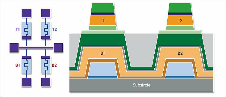
Figure 3: Dmitri Strukov’s team has developed a two layer memristor array that addresses the concept of material implication
Researchers at the Technion in Israel have taken a similar approach with an approach called Imply. Using this logic, each memristor within a regular crossbar can act either as a memory cell or as part of an Imply logic gate in different stages of the operation.
The central argument behind material implication is that the statement ‘if P is true, then so is Q’ equates to ‘Q or not-P’. Although it starts from a place somewhat different from Boolean logic, material implication –coupled with a negation operation – contains the primitives needed to implement the same kind of logic gates as those commonly used in digital design. For example, an XOR gate can be built out of three implication gates: A XOR B = (A IMP B) IMP (B NIMP A).
An issue raised by backers of the STT-MRAM structure is the relatively limited operational lifetime of the ion-transfer and RRAM systems. MRAM, they argue, shows endurance levels several orders of magnitude ahead. But teams working on both approaches see reprogrammable memory-gates as an answer to the problem of dealing with nano-fabrication.
As lithography becomes more challenging, design tends to favour regular arrays – which fits the idea of a crossbar very well. The ability to extend logic into the third dimension should also help improve density once 2D scaling finally runs out of steam. However, as with MRAMs and RRAMs, the density of current-switched devices introduces issues such as leakage between adjacent elements, which could lead to errors in digital systems.
One option is to exploit the ability of domain-wall and RRAM devices to store data in analogue form and accept there will be inaccuracies and device failures. At IEDM this year, a University of Michigan team discussed the performance of a memristor-crossbar array for image processing. They implemented traditional machine-learning algorithms based on functions such as dot-products and found that, even in the presence of stuck-at manufacturing faults, the algorithm performed with acceptable error rates.
Emulating the brain provides another option for failure-prone arrays. Prof Chua argued several years ago that memristor behaviour has parallels to the Hodgkin-Huxley model of the neuron. A number of teams around the world are pursuing these ideas, using memristor arrays to build neuromorphic architectures to work on image and signal-processing problems. As neuromorphic systems need a high level of interconnection between elements, 3D structures will help in their implementation.
People working on the technology like to point to the high energy efficiency of the brain compared to today’s computers and that it is a structure combining compute with memory. Maybe it’s a natural progression.


