Integrated circuits (ICs) are vital in helping to reduce the cost, size and development timescales for many analogue designs. But they can have some significant drawbacks too, such as increased noise and crosstalk, reduced temperature coefficient performance and most importantly, ICs can restrict design flexibility.
Whenever designers are working on high performance applications, such as high-end audio amplifier front ends, medical imaging systems or specialist scientific equipment, they tend to opt for discrete designs to help overcome these limitations. For example: the current sources, sample and hold, and pre-amplification functional blocks within the analogue front-end circuits of a 7 ½ digits bench top multi-meter are almost always designed partially or fully discrete to achieve the highest dynamic performance and the lowest noise.
Despite their potential to improve system performance, most designers avoid attempting to design with discrete components because of the engineering challenges and time involved in using them. These devices require a deep understanding, experience and creativity in electronics and physics, and can also add considerably to design and development timescales and costs compared with integrated solutions.
As a result, many designers steer clear when it comes to complex discrete circuitry, even if it means reduced performance in the final product.
Signal amplification is one of those key areas where discrete solutions almost always win over the use of ICs because they are a much more effective way of achieving very low Enhancing design flexibility noise amplification. For example, the input stages of many high-end audio amplifiers are typically made using fully discrete or hybrid circuits.
Discrete circuits are also extensively used in sensor signal amplification and conditioning where low noise is crucial. In the case of piezoelectric charge output sensors, they are often employed within sensors for dynamic measurement applications such as accelerometers and hydrophone transducers, and where two alternative circuits are typically used for signal conditioning: a voltage mode amplifier circuit or a charge mode amplifier circuit.
Voltage mode amplifiers are capable of linear operation at high frequencies. However, they have a noise floor which may be an order of magnitude higher than the equivalent charge amplified solution. For this reason, low noise high resolution charge amplified sensors are typically used for low amplitude dynamic measurements. Charge mode amplifiers are also routinely employed for amplifying signals from semiconductor detectors, such as photoelectric detectors used for industrial manufacturing applications.
Target parameters
There are three key target parameters within a charge amplifier: low input capacitance, low noise and low input leakage current. In general, op amps have a combination of higher noise and input capacitance when compared to discrete JFETs. For example, the typical input capacitance of a standard FET input op amp may be about 20pF, whereas many discrete JFETs have input capacitances of less than 5pF. Paralleling up a few low noise JFETs can result in an equivalent input noise voltage density lower than any IC can achieve, while at the same time low noise JFETs have the added benefit of often exhibiting low input gate current.
JFETs have relatively high output capacitance which limits the bandwidth but a cascode circuit can be used to overcome this and to achieve higher bandwidths without intermodulation distortion. The cascode topology does this by eliminating the Miller effect that can multiply the effective gate drain stray capacitance and its associated nonlinear effects.
Using a JFET and a cascode topology in a discrete circuit requires a current source and biasing arrangements which increases component count and cost. But it gets even more complicated if the circuit needs to be used within a battery operated portable appliance: where low voltage operation and low power consumption are essential, and the design needs to remain stable and consistent across the operating temperature range without any significant performance degradation.
Figure 1 (below) shows the proposed solution for a charge mode amplifier that uses a method of integrating a discrete current source within a “folded cascode” topology.
Below: Figure 1
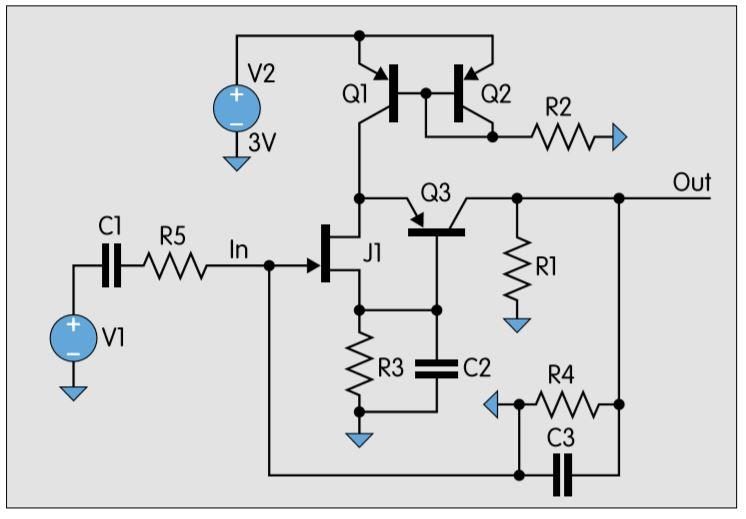
Using this particular implementation of the topology provides a wider voltage swing and incorporating a current source enables low voltage operation. Depending on the JFET selected, the circuit can easily run as low as 2.5V making it feasible to operate from a single lithium thionyl chloride battery cell. The example circuit shown runs at 3V and provides 2.4V output voltage swing before the output starts clipping.
The core of the design is formed around a low noise JFET in a folded cascode circuit. JFET J1 and pnp transistor Q3 together form a folded cascode amplifier. Transistors Q1 and Q2 are configured as a current source to provide a high impedance fixed current source with a large voltage swing. Q1 provides fixed current into J1 and Q3, which is determined by R2 as well as the operating voltage.
Resistors R3 and R1 play a key role in controlling current flow through Q3 and setting biasing points for J1 and Q3. R3 together with C2 creates a biasing point for Q3 and J1, while J1’s biasing point also depends on R1.
Using this interlaced biasing approach helps to reduce component count and simplifies the circuit.
Although the current flowing through the circuit is almost proportional to the operating voltage, the performance is not affected within 2.5 to 5V voltage range. The feedback loop is created from the output of Q3 and routed back to the J1 input via C3 and R4.
However, introducing an IC to create a hybrid version of the circuit can deliver further benefits including design simplification, reduced output impedance, increased bandwidth or improved reliability.
Figure 2 (below) shows one potential implementation where adding a standard low cost and low power op amp IC to the output stage can reduce output impedance and increase bandwidth. This op amp, typically costing a few cents, has a standard noise density so its noise contribution is negligible as it has unity gain; and C4 is required to increase stability of the circuit and prevent oscillation.
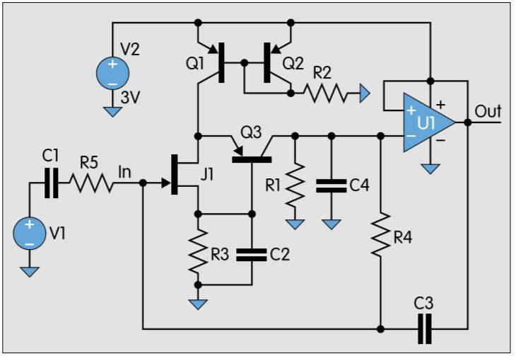
Above: Figure 2: Folded cascode amplifier with op‐amp buffer
The final circuit as shown provides 34dB gain in the 10Hz to 4kHz range and achieves 5μV output noise for the same frequency range, while consuming only 0.2mA from a 3.6V source (e.g. a lithium battery). Figure 3 shows the output noise spectral density for the design.
The total BOM cost for the hybrid circuit is still low, at around US $0.3 for 10k manufacturing volume: whereas any alternative solution taking a fully integrated approach would either have a higher BOM cost or require higher power consumption for the same output noise performance.
The circuit which has been developed can be used in a variety of applications where low noise, low cost and low power are all essential requirements. However, as it has been designed with discrete components it can also be easily modified depending on the application. For example: increasing the power consumption and paralleling up multiple low noise JFETs can significantly reduce the output noise.
The input referred noise of the circuit is currently around 3nV/√Hz at 1kHz but it can be lowered down to 0.5nV/√Hz using these techniques.
Different methods can also be applied to help further reduce power consumption if required, and to exploit the inherent flexibility within the circuit that would be almost impossible to achieve with a design relying solely on the use of ICs.
Author details: Tolga Aydemir is an electronics engineering consultant at 42 Technology.