
Successful wireless standards such as Wi-Fi, Bluetooth, and protocols like ZigBee that use standardised IEEE 802.15.4 radio layers, have enabled the emergence of wireless System-on-Chips (SoCs) that relieve product-development teams of many RF design challenges.
Armed with a reference design from the SoC vendor, which answers the few remaining questions surrounding component selection, layout and PCB design, application-focused OEMs can begin developing new wireless products with minimal in-house RF knowhow.
When using a wireless reference design, it is extremely important to replicate the design exactly. Any deviation risks detuning the system or creating difficulties in gaining approvals. In practice, reproducing the reference exactly may be impossible due to constraints on size or form-factor and reference designs tend to focus only on the RF section, not the surrounding system circuitry.
With an understanding of board-layout best practice, non-RF engineers can make better decisions when adapting a reference design or fine-tuning their own board designs to optimise RF performance.
Keeping connecting wires and PCB traces short is a widely-known RF-design principle. If a reference design must be adapted to fit within a confined space, changing the distances between components can introduce parasitic inductances due to the different circuit board trace lengths. A different substrate thickness or dielectric constant, or the gaps between traces, can introduce parasitic capacitances. Changing the spacing or orientation of components relative to one another can affect signal couplings, while changing component types or sizes can introduce different parasitic capacitances.
Poor design choices can also cause detuning of the matching and filtering network and can also detune the load of the crystal. This network is needed to maximise radiated power at the fundamental frequency and minimise any dissipated losses from harmonic and other spurious frequencies. 2.4GHz RF circuits operating at transmitter-power levels above 13dBm typically require a 4-element network of capacitive and inductive components as shown in Figure 1. In receive mode, the receiver uses the same impedance-matching network to achieve maximum sensitivity.
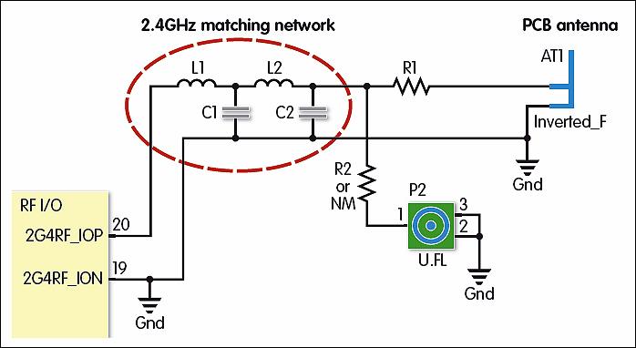
Figure 1. 4-element matching and filtering network for 2.4GHz transmitter
Incorrect modifications to this filtering and matching network can have consequences and potentially a frequency offset between different boards.
Design decisions beyond the RF section of the circuit board must also be considered. From an RF radiation perspective, factors such as the ground plane and its size will affect the power of the transmitted signal, especially when using a monopole-type antenna. The shielding effect of the ground plane, as well as non-RF traces, will also affect the level of radiated spurs, which need to be kept within EMC limits.
Layout and PCB design
If the reference design cannot be replicated exactly, some basic component layout and PCB-design guidelines can help minimise performance degradation. Figure 2 shows example guidelines for the layout of a 2.4GHz radio board.
Starting with the matching network, placing the first component as close as possible to the Tx output pin of the RF IC can help minimise the effects of any necessary changes in signal trace length. The remaining matching network components should also be placed close to each other to minimise other trace inductance and any PCB parasitic capacitance to ground. Ideally the trace width used to connect these components should be the same as the pad width. This is typically 0.5mm for 0402-sized chip components.
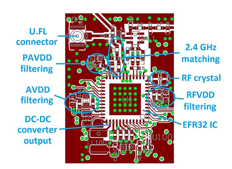
Figure 2. Layout of a 2.4 GHz EFR32 radio board showing key circuit areas
Positioning decoupling capacitors correctly on supply pins is vital. The lowest value bypass capacitors filter out signals around the fundamental signal frequencies and need to be placed closest to the IC pins. Good grounding using multiple vias to the ground plane is always recommended. Bypass capacitors with values around 100nF will suppress clock signals in the range of tens of megahertz, which could otherwise be up-converted within the chip, causing unwanted spurs around the carrier frequency. The largest value capacitors are intended to filter out the interference coming from switching power supplies, which will typically be around several hundred kilohertz. These can be placed further from the supply pins.
Placing the crystal as close to the RF IC as possible minimises via parasitic capacitances as well as any frequency offsets. The case of the crystal should be connected to ground using multiple vias to avoid radiation from ungrounded parts as any metal left unconnected and floating may act as an unwanted radiator. Using an isolating ground metal between the crystal and VDD traces will avoid any detuning effects on the crystal caused by the supply and will equally avoid the leakage of crystal or clock signals, and their harmonics, to the supply lines.
Good ground connections are vital. Ensuring thick traces near the ground pins of capacitors can improve the grounding effects of the thermal straps (provided for cooling) and minimise the series parasitic inductances between the ground pour (where unused areas of a board are filled with copper that is grounded) and the ground pins. Adding extra vias close to the ground pins of capacitors will further help to reduce these effects.
The exposed pad footprint for the paddle of the RF IC should use multiple vias to ensure good grounding as well as a good heat sink capability. In the layout shown in Figure 2, there are 25 vias for a 7mm x 7mm-sized IC package, each 0.25mm in diameter. If possible, the paddle grounds should be connected to the top-layer ground metal to further improve RF grounding. This may be accomplished with diagonal trace connections through the corners of the IC footprint. Signals, especially higher frequency harmonics, can sometimes be coupled between the ground connections of nearby filter capacitors.
Close to the matching network, a separation of at least 0.5mm between traces or pads and the adjacent ground pours helps to minimize parasitic capacitances and reduce detuning effects. With a 4-layer PCB, the first inner layer beneath the top layer should be filled with a continuous ground metal under the RF IC and the matching network. This will ensure a good low-impedance signal path to the RF IC’s ground. Moreover, excluding wiring from this region prevents any coupling effects with the matching network. The board design should also avoid blocking the ground return path between the ground vias of the transmitter/receiver matching network and the ground vias of the RF IC paddle, to provide a clear pathway for return currents through the ground plane back to the RF IC.
Finally, regarding the RF section specifically, connections to distant RF components such as the on-board antenna or antenna connector should be made using 50-Ohm grounded coplanar transmission lines. This will reduce sensitivity to any variation in signal caused by the PCB and will also reduce unwanted radiation and coupling effects. The use of transmission lines can be seen in Figure 3.
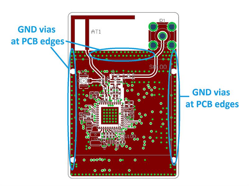
Figure 3. Complete board layout showing transmission lines and ground vias at the PCB edge.
Best Practice
While, as a minimum, it is good practice to have a large continuous ground metallisation around the area of the RF section of a PCB, better performance may be obtained by applying this technique to the entire PCB. To achieve a good RF ground, the RF voltage potentials should be equal across the entire ground area. This helps maintain proper filtering on power supply lines, and provides a good ground plane for monopole-type antennas. Gaps should be filled with ground metal, and the resulting sections on the top and bottom layer should be connected using as many vias as possible.
To reduce harmonic radiation caused by fringing fields, multiple grounding vias should be deployed at the edges of any ground metal area, especially at the edge of the PCB and around supply traces, as shown in Figure 3. In a board design with more than two layers, all the wires or traces should be placed in one of the inner layers, especially supply traces, and the entire top and bottom layers should contain as much continuous ground metallization as possible to reduce any radiation from these traces. It is also recommended to avoid placing supply traces close to the PCB edge.
Although today’s wireless SoCs and supporting reference designs simplify wireless-system design, taking time to understand component layout and board design principles can help create products that stand out among the competition.
Krisztián Kovács is Senior Director, Applications Engineering, Silicon Labs


