
Figure 1 shows a switching regulator that can generate a lower voltage from a high voltage. In this type of circuit, the bypass capacitor (CBYP) is especially important. It has to support the switched currents on the input path so that the supply voltage is stable enough to enable operation.
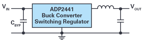
Figure 1
Because the input capacitor in a buck converter is part of the critical paths (hot loops) for this topology, CBYP has to be connected with as little parasitic inductance as possible. Thus, the placement of this component is important.
The left side of Figure 2 shows a layout that is not very useful. Thin traces are routed to the bypass capacitor. The current flowing into the voltage converter also does not flow directly from the bypass capacitor. The bypass capacitor is only connected with additional thin contacts. This increases the parasitic inductance of the capacitor and reduces the effectiveness of this component.
A suggested layout in which the effectiveness of the bypass capacitor is very high can be seen on the right side of Figure 2. The connection is made with very little parasitic inductance. It can also be seen that the pinout of the component being supported, for example, a switching regulator, has an effect on the board layout options. On the right side of Figure 2, the VIN and GND pins are closer together than in the poor example on the left side. This results in a smaller loop area between the bypass capacitor and the integrated circuit.
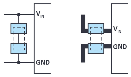
Figure 2
Because the bypass capacitors should be connected with as little parasitic inductance as possible, it is recommended that they be placed on the same board side as the switching regulator is on. However, there are applications in which decoupling with a bypass capacitor is only possible on the bottom side of the board. One example is when there is not enough space for a large decoupling capacitor. In such cases, vias are used to connect the capacitor. Unfortunately, they have a few nanohenries of parasitic inductance. To keep this connection impedance as low as possible, various proposals for connection are given, as shown in Figure 3.
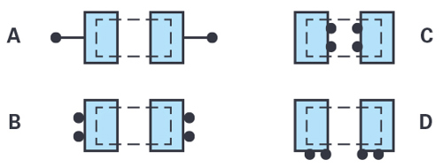
Figure 3
Version A is not particularly advantageous. Here, thin traces are used between the vias and the bypass capacitor. Depending on where on the other side of the board the paths to be supported run, the geometrical arrangement can also lead to increased parasitic inductance.
In version B, the vias are brought much closer to the bypass capacitor, thus this is a much better connection. Also, two vias are used in parallel. This reduces the total inductance of the connection.
Version C is a very good connection in which the loop area for the connection can be very small, thus there is only a very small amount of parasitic inductance here. However, with very small bypass capacitors and low-cost manufacturing processes, vias underneath components are not possible or permissible.
Example D can be an interesting connection. Depending on how a specific ceramic bypass capacitor is designed, lateral connection to the board can represent the path with the lowest parasitic inductance.
Placement of bypass capacitors on the board is very important for achieving the greatest possible effectiveness for these components. Here, connection with as little parasitic inductance as possible is important. The most suitable connection uses the same side of the board as the circuit being supported is on, as shown in Figure 2.
In exceptional cases in which connection of the bypass capacitor on the back of the board is necessary, a connection with as little parasitic inductance as possible, as shown in examples B, C, and D in Figure 3, should be selected.
Author Details: Frederik Dostal, Field Applications Engineer, Analog Devices
Frederik Dostal can be reached at frederik.dostal@analog.com
This is the third in a series of Design Tips from ADI.
Follow the links below to read:
Design Tips from ADI: What actually is a hot loop?
Design Tips from ADI: Overvoltage protection for sensitive electronic signal inputs


