
But in sensor nodes and other low-energy systems where battery lifetime is a critical concern, often the enemy of the circuit designer is the slow quiet leak. And this is where analogue and mixed-signal subsystems often reign. While the processor and memory sleep, the analogue I/O and clock circuits need to keep running for long periods because they are the eyes and ears of the product.
A further problem for mixed-signal designers is trying to work out ways to get high quality signals with low noise when the voltage rails they deal with are now reliably less than 1V. This affects circuits such as op amps as the voltage drop of any transistor in the output path restricts how many of them can be used and whether the devices can operate fully. The number drops quickly to just two. One option is to simply to never let them switch fully.
Forty years ago, two researchers working in Switzerland showed how to model transistors that never fully switch on in usable analogue circuits, such as oscillators for low-energy wristwatches, as well as bandpass amplifiers. The ‘weak inversion’ topologies described by Eric Vittoz and Jean Fellrath of the Centre Electronique Horloger in Neuchatel now fall under the banner of sub-threshold and near-threshold design. The technique can deliver impressive energy savings, as long as you do not want to process data in a hurry – with very low swings in voltage, transistors become far less responsive.
Weak-inversion design sat on the sidelines for several decades because other techniques delivered a better performance:cost ratio. Renewed interest in sub-threshold design arrived with concern over the power consumption of digital circuits, though their application has been limited because of their performance problems. Now, sub-threshold is back as part of a growing portfolio of analogue design techniques that try to attack the dual problems of falling voltages and the need to save power in micro power sensors.
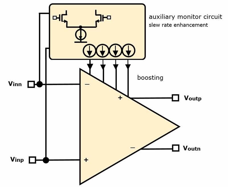 Figure 1: General block diagram of an op amp with slew rate enhancement
Subthreshold circuitry makes it easier to deal with the tiny outputs of energy sources such as small solar cells and vibration harvesters. Many of these find it difficult to generate even as much as 1V of output. In order to handle such low voltages, novel techniques and transistors are needed. Take a simple function such as a bandgap voltage reference. Traditionally, these were constructed using bipolar devices – CMOS engineers could use parasitic bipolar transistors to do the same job. But low voltages call for native MOS versions.
A decade ago, researchers from the University of Pisa developed a sub-1V nanowatt voltage reference that coupled a transistor operating in the subthreshold region with another in full saturation. But a constant consumption of almost 70nW just for a single analogue function running for long periods of time easily adds up to a significant proportion of the total energy needs of a micropower sensor.
An option proposed by a group led by David Blaauw at the University of Michigan is to take an I/O-capable transistor, which works at high thresholds, and stack that on top of a so-called zero-threshold voltage transistor: one that switches on fully at less than 100mV. By carefully adjusting sizes relative to each other, their temperature dependencies cancel out. This provides a stable voltage reference and overcomes one of the biggest problems of subthreshold design: its much higher susceptibility to process variation. By choosing maximum-length devices, the leakage of the of the zero-threshold transistor can be kept low. In a test chip fabricated in a 130nm process, the voltage reference consumed slightly more than 2pW and occupied a silicon area of 1350µm2.
Zero-threshold transistors are not the sole preserve of IC designers, however. Advanced Linear Devices recently launched a device that puts four zero-threshold PMOS transistors onto a discrete device. Robert Chao, CEO of ALD, says the devices were developed to support applications in energy harvesting, as well as signal-conditioning circuits for IoT sensors.
Although variation is an issue of subthreshold design, Blaauw and his colleagues have found aspects of weak-inversion transistor operation can work in favour of some types of analogue circuit. Transconductance improves in the subthreshold region as long as parasitic capacitances can be kept low. Various teams have harnessed this idea by revisiting the telescopic cascode amplifier, which stacks multiple MOS transistors on top of each other. Conventionally, the architecture limits the voltage swing of each, but this is less of a problem in a circuit intended for transistors that are operating deep in the subthreshold zone.
To overcome the problem of process variation, amplifiers for slow-moving signals take advantage of pseudo-resistors constructed from transistors. Circuits not only use these pseudo-resistors to tune the circuit dynamically, but also provide very high resistance values that are difficult to achieve with entirely passive structures on an IC.
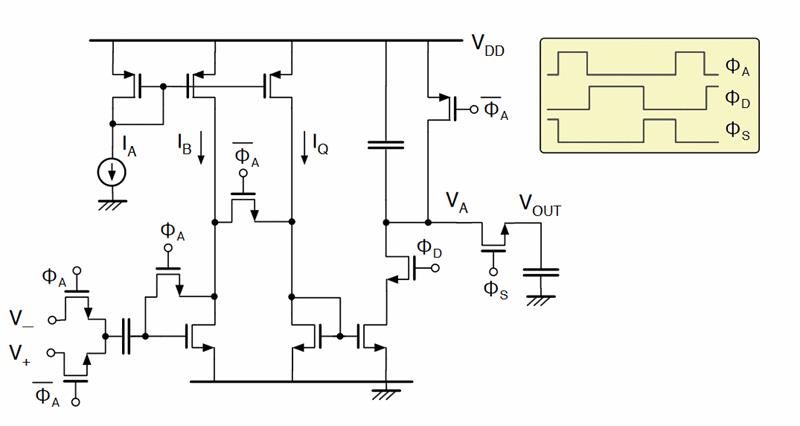
Figure 2: Block diagram of a sampled data op amp.
Near-threshold operation is not the only possibility for low-voltage analogue. However, circuit designers have to cope with the limited gain of conventional circuits or suffer high leakage power. One option is to use assistance circuitry to modify behaviour dynamically and so only incur high current levels when necessary.
One approach used by Franco Maloberti and colleagues from the University of Pavia is to have an auxiliary circuit that looks at the incoming signal and adjusts the operation of the op amp so that it can respond better to increases in slew rate. Another approach they have pursued, along with colleagues from the University of Istanbul, is the option is to move even further into the territory of sampling that began with chopper-stabilised amplifiers. The result is a sampled op amp. While the concept only works for low-bandwidth signals of up to a couple of thousand hertz, it greatly reduces the quiescent and operating power. Implemented on a 180nm process, a single-ended version of the sampled-data op amp showed a gain of more than 40dB and a bandwidth of 2.5kHz, while consuming just over 60nW.
There is also some good news for SoC designers in the push to smaller geometries. The core performance of the core transistor is, according to designers working on these advanced nodes, much better than equivalent planar transistors. Problems arise in other ways. One, which has proved less important in reality, is the quantised nature of the finFET because the effective width is set by the fin count. In practice, the improved matching performance outweighs the problems.
The finFET is far from free of issues. There are problems with parasitics that stem from the complex interactions between the fins and the metal interconnect around. And though density is rarely an issue in analogue circuits, the need to follow the strict routing requirements of nanometre processes to avoid difficulties with manufacturing and variation caused by stresses around the edges of transistor arrays makes layout much more of an iterative and time-consuming process. Even with such problems, the drive below 1V continues to yield viable analogue and mixed-signal designs.


