The markets for augmented and virtual reality (AR/VR) are thriving, with market researcher IDC predicting demand for both will reach $17.8billion in 2018.
While VR is making rapid inroads into the consumer electronics world, AR is poised to have a similar impact in industry – and PCB design is one of the potential beneficiaries, where it could address issues such as fitting electronic packages into unconventional shapes, ensuring circuit connections work properly and reducing the time-consuming process of place and route.
Unlike VR, which fully immerses the user in a digital world, AR sees digital content overlaid onto the existing reality. Virtual objects are oriented so they appear to have real places in the world.
If electronic design could benefit from AR, the question is why hasn’t it been put into practice already?
“People are solving software issues where there is high value,” David Harold, VP marketing and communications at Imagination Technologies, said. “They will pay for the issues they want to be resolved, such as ones that aid protection and health.”
Harold highlighted several areas where he believes AR could be used in the future. The first he labelled ‘procedure’; the idea that a designer could flick between the finished, virtual version of a board and the real-life work-in-progress. He suggested this could help the designer establish what still needs to be done and remind them of the finished article.
The second area is ‘non-distraction’. “People forget how finely detailed some of the work we do is,” he said. “The ability to have a set of virtual instructions in your field of vision, so you don’t have to keep manually turning pages would be very useful.” He described a theoretical system where a user could access a ‘tunnel’ view, in which areas of their vision could be darkened in favour of particular highlighted areas.
He also proposed combining AR with artificial intelligence (AI), offering a scenario in which an AR AI-enabled system could recognise the parts a designer was working on and provide optimisations. This imagined system could suggest alternatives, identify missing elements, offer solutions others have solved and shared previously, as well as search and highlight stress and failure points in a design.
The ability for an AR system to distinguish between necessary and needless motions would also be crucial in electronic design. Real world movement isn’t always logical, so a system would have to be intelligent enough to categorise these, so to avoid delay and error.
“Ultimately,” said Harold, “the technologies being developed in the health and consumer markets will start to trickle through to other industries.”
Heather Macdonald Tait, marketing communications specialist at Ultrahaptics, believes one reason why AR has not been implemented in electronic design is due to the ‘chicken and egg situation’ between software and hardware development. “We need the right tools to develop content,” she explained. “But we also need the hardware to support it and this has affected market acceptance.”
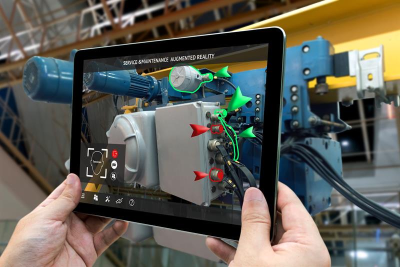
| Above: AR is already being used in an industrial setting for tasks such as fault-finding, but has yet to reach its full potential in PCB design |
Ultrahaptics’ technology enables haptic feedback in mid-air. Using a speaker array controlled by an FPGA and a microcontroller, ultrasound is emitted at 40kHz. The system controls when each speaker fires, creating an array of pressure points which enables a user to ‘feel’ a virtual object.
“Until we add a mechanism for interacting in a collaborative way,” Dr David Fee, an Ultrahaptics applications engineer, added, “I don’t think we’re opening up the full potential of AR and VR. We believe we are opening that potential with haptics and it’s up to people using this tool to leverage the technology.”
Altium is also experimenting with ways AR can be used in design. In previous tests, it linked 3D glasses to the 3D PCB editor view in its software, so the designer’s facial position could augment the control of the PCB design workspace. However, it was never carried beyond experimental phase because it was hard to establish any true value or efficiency gains.
“It’ll take time for electronic engineers to think of ways in which AR could help them day-to-day. We’re waiting for some better technology,” Ben Jordan, senior manager product and persona marketing at Altium, said. “It’s like the laser; they didn’t know what to do with it at first and now it’s everywhere.”

Jordan believes the answer could lie in the creation of light emitting touchscreens. He imagines a technology where an image would be projected in front of the user, allowing them to interact through gestures. “One day, we’ll design software into transparent touchscreens and people will be able to hold them over a prototype of a board and plug it in. There will be test applications where designers can verify their work in prototype against the actual design in the software simultaneously.”
He also explored the idea of training and using AR with simulation software. He suggested augmented PCBs could be used in the future to reduce cost and wastage of material used in current training methods, as well as for replicating magnetic and electric fields generated by a product as alternative way to ensure a product would meet regulations.
| "Much like the integration of 3D into PCB design would have been in the late 1980s, AR is a solution to problems we probably don't yet have." Ben Jordan, senior manager product and persona marketing, Altium |
“AR could potentially play a role in making the electronics design more intimate with industrial design,” Jordan added. “For example, a product designer may create a clay mockup of the product idea and then the electronics designer may use AR views of that mockup combined with the clusters of parts in the PCB design software in real-time to begin shaping the PCBs and figuring out where some of the bulkier components would fit inside of it, or make alternative part choices to replace them with smaller components.
“Much like the integration of 3D into PCB design would have been in the late 1980s, AR is a solution to problems we probably don’t yet have,” Jordan ventured. “Today, everyone knows you must have 3D PCB design viewers at a bare minimum for efficient design, but that was not so obvious 20 years ago. As the technology and our design patterns evolve, it will become more apparent,” Jordan ventured.
“I could see that AR will become far more useful for PCB design as 3D MID technology becomes mainstream,” he continued. MIDs – Mechatronic Integrated Devices – are 3D bodies with integrated circuit structures. “With the 3D MIDs, you want to take a plastic or clay mockup of the moulded shape and, with the CAD and an AR camera view, in 3D, superimpose the track routing and component placements.”
“But maybe that isn’t necessary,” he countered. “You could simply bring in the STEP or Parasolid model of the MID design into the editor environment, place the parts and route them. Only time will tell.”
While AR may have a place in electronic design in the future, it seems that progress needs to be made in developing suitable hardware. Until then, AR in electronics may remain a mere gimmick.


