
They are usually used to sense temperature, flow, fill level, pressure, and other physical quantities, which are then converted to high resolution digital information and forwarded for further processing via software.
Such systems require increasingly more precision and higher speeds. These data acquisition systems are composed in part of analogue-to-digital converters (ADCs), the performance capabilities of which have a decisive effect on the system. However, the input driver of the ADC also impacts the overall accuracy.
The driver has the task of buffering and amplifying the input signal. In addition, it must increase the input signal or generate a fully differential signal to cover the input voltage range of the ADC and meet its common-mode voltage requirements. The original signal must not be changed in the process.
Programmable gain instrumentation amplifiers (PGIAs) are often used as input drivers. Here we present a coordinated combination of input driver and ADC with which extremely accurate conversion results can be achieved and, thus, high quality data acquisition systems can be built.
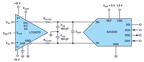
Figure 1. Example of a circuit for driving a precision ADC.
An example of a suitable PGIA for high precision data acquisition systems is the LTC6373. It offers, apart from fully differential outputs, a high dc accuracy, low noise, low distortion (see Figure 2), and a high bandwidth of 4MHz with a gain of 16. ADCs can be driven directly with it, which is why it is suitable for numerous signal conditioning applications, among others.
The circuit in Figure 1 shows an example using the LTC6373 to drive a precision ADC - specifically, the AD4020, a 20-bit ADC with 1.8MSPS.
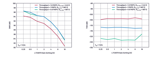
Figure 2. SNR (left) and THD (right) for driving the AD4020 with the LTC6373.
In the circuit, the LTC6373 is dc-coupled at the input and at the output, thereby eliminating the need for a transformer to drive the ADC. The gain can be set between 0.25V/V and 16V/V via pins A2/A1/A0. In Figure 1, the LTC6373 is used in a differential input to differential output configuration with a symmetric supply voltage of ±15V. Alternatively, the inputs can be operated asymmetrically if a differential output is required.
In Figure 1, the output common-mode voltage is set via the VOCM pin to VREF/2. Through this, a level shift in the outputs of the LTC6373 is achieved. Each of the outputs on the LTC6373 varies between 0V and VREF (out of phase), so there is a differential signal with an amplitude of 2× VREF at the ADC inputs. The RC network between the outputs on the LTC6373 and the ADC inputs forms a single-pole low-pass filter, which reduces current peaks that arise when switching the capacitors at the ADC inputs. At the same time, the low-pass filter limits the broadband noise.
Figure 2 shows the signal-to-noise ratio (SNR) and the total harmonic distortion (THD) of the LTC6373, which drives the AD4020 SAR ADC (in high-Z mode) over its entire input voltage range (10V p-p). The best results are achieved with a throughput of 1.8MSPS and a filter resistance (RFILTER) of 442Ω. At 1MSPS or 0.6MSPS, an RFILTER of 887Ω is recommended by the manufacturer.
The LTC6373 can drive most SAR ADCs with differential inputs and does not need its own ADC driver. However, in some applications, it can be advantageous to use a separate ADC driver between the LTC6373 and the precision ADC to simplify the transients of the LTC6373 and improve the linearity of the signal chain.
Conclusion
The circuit shown in Figure 1 is optimised for fast, high precision data acquisition systems. Thus, with the outstanding properties of the LTC6373, the full performance capabilities of connected sensors can be exploited.
With the online tool ADI Precision Studio and especially the ADC Driver Tool included in it, Analog Devices offers additional support in the design of such amplifier stages, filters, and linear circuits.
For more information, please go to www.tools.analog.com/en/precisionstudio
Author details: Thomas Brand, Field Applications Engineer, Analog Devices
He can be reached at:
This is the thirteenth in a series of Design Tips from ADI.
Follow the link below to read:
Design Tips from ADI: What actually is a hot loop?
Design Tips from ADI: Overvoltage protection for sensitive electronic signal inputs
Design Tips from ADI: Bypass Capacitor and Coupling Capacitor: Stabilising Voltage the Right Way
Design Tips from ADI: Temperature Measurement Technologies
Design Tips from ADI: Generation of Low Noise Voltages
Design Tips from ADI: When the Flyback Converter reaches its limits
Design Tips from ADI: When the Supply Voltage is Dynamic
Design Tips from ADI: Building Programmable Oscillators
Design Tips from ADI: Monolithic Switching Regulators
Design Tips from ADI: Switching Frequency Considerations
Design Tips from ADI: Reliable power up and power down
Design Tips from ADI: Improving dynamic loop response


