
If these signals exhibit a simple, periodic waveform, such as with sine, square, or triangular waves, the generators are called function generators. They are often used to check the function of electrical circuits or assemblies.
A defined signal is applied to the input and connected at the output to a corresponding measuring device (for example, an oscilloscope). It can then be evaluated by the user. In the past, the challenge usually consisted of designing the output stage. A description of how to design a small and inexpensive output stage with a voltage gain amplifier (VGA) and a current feedback amplifier (CFA) is described in this article.
Typical signal generators offer output voltages in the range of 25mV to 5V. To drive loads of 50Ω and higher, powerful discrete components, multiple components in parallel, or expensive ASICs are typically used on the output side. Internally, there are often relays that allow devices to switch between different amplification or attenuation levels and thus adjust the output level. Through the required switching of the relay for various gains, discontinuous operation arises to a certain extent. A simplified block diagram is shown in Figure 1.
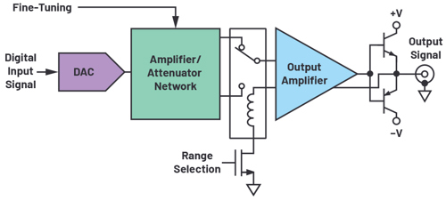
Figure 1. Simplified block diagram of a classic signal generator output stage.
With newer amplifier ICs, loads can also be driven directly without any internal relay. The design of the generator output is thereby simplified and the complexity and costs are lowered. The two main components of such an output are building a powerful output stage, which delivers high speeds, high voltages, high currents, and a variable amplifier with continuous linear fine-tuning capabilities.
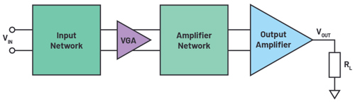
Figure 2. Simplified block diagram of a signal generator output stage with VGA.
First, the original input signal must be amplified or attenuated through a VGA. The VGA’s output signal can be set to a desired amplitude independent of its input signal. For an output amplitude, VOUT , of 2V at a gain of 10, for example, the output amplitude of the VGA must be regulated to 0.2V. Unfortunately, many VGAs represent the bottleneck due to their limited gain range. Gain ranges greater than 45dB are quite rare.
With the low power VGA AD8338, Analog Devices enables a programmable gain range from 0dB to 80dB. Thus, under ideal conditions, output amplitudes between 0.5mV and 5V can be programmed continuously for signal generators without the need for additional relays or switched networks.
Through the omission of these mechanical components, discontinuities can be avoided. Because digital-to-analogue converters (DACs) and direct digital synthesis (DDS) components often have differential outputs, the AD8338 offers a fully differential interface. In addition, via a flexible input stage, any asymmetries in the input currents can be compensated through an internal feedback loop.
At the same time, the internal nodes are kept at 1.5V. Under normal conditions, the maximum 1.5V input signal generates a current of 3mA at input resistances of 500Ω. With higher input amplitudes - for example, 15V - a higher resistance would be required directly on the input pins. This resistance is sized in such a way that the same current of 3mA results.
Many commercial signal generators deliver a maximum effective output power of 250mW (24dBm) at a load of 50Ω (sine wave). However, this is often inadequate for applications with higher output powers, as are required, for example, for testing HF amplifiers or generating ultrasonic pulses. For this reason, current feedback amplifiers are also used. The ADA4870 enables a drive current of 1A at an amplitude of 17V on the output side for a supply voltage of ±20V. Sine waves can be generated under full load up to 23MHz, which makes them ideal front-end drivers for universal arbitrary waveform generators.
To optimise the output signal swing, the ADA4870 is configured with a gain of 10, thus the required input amplitude is 1.6V. However, because the ADA4870 has a ground-referenced input, but the upstream AD8338 has a differential output, a differential receiver amplifier for differential-to-ground-referenced conversion should be connected between both parts.
The AD8130 offers a gain-bandwidth product (GBWP) of 270MHz and a slew rate of 1090V/µs, which is a very good fit for this application. The output of the AD8338 is limited to ±1V, so the intermediate gain of the AD8130 should be designed to be 1.6V/V. The overall circuit configuration is shown in Figure 3. It offers a bandwidth of 20MHz at an amplitude of 22.4V (39dBm) and a load of 50Ω.
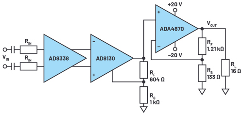
Figure 3. Simplified circuit of a discretely designed signal generator output stage.
Through the combination of a high power VGA (AD8338), a powerful CFA (ADA4870), and a differential receiver amplifier (AD8130), a compact high power signal generator output stage can be built relatively easily. It outshines traditional output stages through its higher system reliability, higher service life, and lower costs.
Author details: Thomas Brand, Field Applications Engineer, Analog Devices
He can be reached at:
This is the fourteenth in a series of Design Tips from ADI.
Follow the link below to read:
Design Tips from ADI: What actually is a hot loop?
Design Tips from ADI: Overvoltage protection for sensitive electronic signal inputs
Design Tips from ADI: Bypass Capacitor and Coupling Capacitor: Stabilising Voltage the Right Way
Design Tips from ADI: Temperature Measurement Technologies
Design Tips from ADI: Generation of Low Noise Voltages
Design Tips from ADI: When the Flyback Converter reaches its limits
Design Tips from ADI: When the Supply Voltage is Dynamic
Design Tips from ADI: Building Programmable Oscillators
Design Tips from ADI: Monolithic Switching Regulators
Design Tips from ADI: Switching Frequency Considerations
Design Tips from ADI: Reliable power up and power down
Design Tips from ADI: Improving dynamic loop response
Design Tips from ADI: Driving High Precision Analogue-to-Digital Converters


