
The need for 10, 20, or more voltages is not unusual. Added to this are voltage domains that have the same voltage level but must be generated separately as domains - that is, these voltages must be generated twice. An example is the implementation of two identical voltages to supply an analogue and a digital load. This separation prevents mutual interference and supplies energy to various loads at various times.
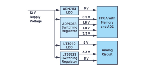
Figure 1. Typical electronic system requiring eight voltages.
Figure 1 shows the block diagram of a system with numerous different voltage domains. These voltages are generated with individual switching regulators and linear regulators. Selection of the individual voltage converters strongly depends on the conversion efficiency required, the voltage to be generated, and, especially, the current consumed by the respective loads. As a result, the individual voltage converter designs vary greatly.
Additionally, the delays of the individual voltages coming up will be different for each converter. This results in uncontrolled ramp-up in the different voltage domains, which can lead to functional problems and damage to the system.
Thus, generally, a reliable power-up sequence is required to ensure that each voltage reaches its target value at the right time. Often, a specific power-down sequence must also be followed for shutdown.
In systems with multiple supply voltages, the ability to monitor the different voltages may be important. What appears trivial in systems with just two voltage domains becomes very complex for numerous voltages. For this reason, many sequencer devices also have a built-in supervisor or voltage monitoring function.
Figure 2 shows an ADM1186-1 analogue sequencer IC. It can control and monitor four voltage domains. Power-up and power-down of the voltages are performed through control of the enable (on/off) pins on the respective voltage converters. The turn-on times of the voltage converters can be adjusted by means of time delays using small capacitors. The respective output voltages are monitored via the corresponding monitor pins. When all voltages have been established, the sequencer circuit generates a power-good signal.
Analogue sequencing solutions such as the ADM1186-1 are easy to use. They have all the functions required for systems with multiple voltages. They differ from digital sequencers in that they have less complex designs and require fewer digital monitoring functions in the system. For example, they can do without a PMBus or similar protocol.
In the example system shown in Figure 1, eight voltage domains are utilised. How can sequencing and monitoring be done for a system with more than four voltage domains? Multiple ADM1186-1 circuits can be combined in a sequence for this and any number of ADM1186-1 sequencers can be wired together.
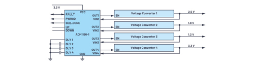
Figure 2. An ADM1186-1 analogue sequencer solution for monitoring up to four voltage converters.
Numerous examples of this type of sequencing with coupled individual sequencers can be found on the market. However, the ADM1186-1 stands out because it also supports complete sequencing during power-up, as well as power-down when used in a linked application, as shown in Figure 3. Comparable solutions can offer the possibility of linking various sequencer ICs, but they only offer controlled ramp-up of the individual voltages, not controlled down-sequencing - that is, power-down of the voltages, in such a daisy-chain constellation.
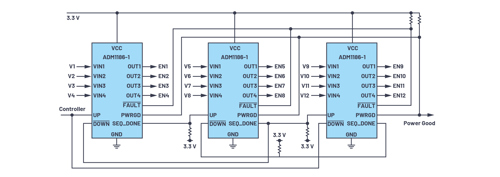
Figure 3. Multiple ADM1186-1 devices chained together for sequencing the power-up and power-down of 12 voltages.
Reliable, monitored power-up and power-down are important in many modern systems and can be realised flexibly and with little development effort using solutions such as the ADM1186-1.
Author details: Frederik Dostal, Field Applications Engineer, Analog Devices
He can be reached at:
This is the eleventh in a series of Design Tips from ADI.
Follow the link below to read:
Design Tips from ADI: What actually is a hot loop?
Design Tips from ADI: Overvoltage protection for sensitive electronic signal inputs
Design Tips from ADI: Bypass Capacitor and Coupling Capacitor: Stabilising Voltage the Right Way
Design Tips from ADI: Temperature Measurement Technologies
Design Tips from ADI: Generation of Low Noise Voltages
Design Tips from ADI: When the Flyback Converter reaches its limits
Design Tips from ADI: When the Supply Voltage is Dynamic
Design Tips from ADI: Building Programmable Oscillators
Design Tips from ADI: Monolithic Switching Regulators
Design Tips from ADI: Switching Frequency Considerations


