
But to what exactly does a hot loop refer?
Currents are always switched in switching regulators. These currents are usually relatively high. Whenever a current flows, it generates a magnetic field. If high currents are rapidly switched, an alternating magnetic field is generated. Also, if currents are switched through a certain parasitic trace inductance, a voltage offset is created. The current can capacitively couple into adjacent circuit parts and increase the noise radiation of a power supply. In summary, we can state that the main cause of noise in a switched-mode power supply are the switched currents.
Figure 1 shows a simple buck converter topology. All lines carrying a continuous current are shown in blue. All lines that rapidly switch currents are shown in red.
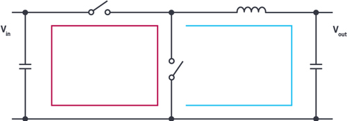
Figure 1. Paths with continuous current shown in blue and switched current shown in red.
The red paths in Figure 1 are the critical paths. They look like a current loop and are hence referred to as a loop. Hot loop means that this loop is especially critical because it involves rapidly switching currents. If we take a closer look at this loop, we can see that the red loop in Figure 1 never has any real current flowing since both of the switches are never turned on at the same time. It is only a combination of individual lines through which current flows at certain times and no current flows at other times. In Figure 2, arrows showing the direction of current flow are added to the individual connecting lines. Also, symbols showing at which time in a period current flows are given. At other times, no current flows through the conductor.
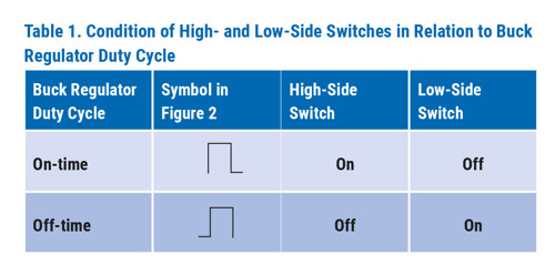
Table 1 shows when each red trace in Figure 2 conducts current and when they do not conduct current. During the on-time of the buck regulator duty cycle, the high-side switch is on, the low-side switch is off, and we see the current flow from the input capacitor, through the high-side switch, but no current flows through the low-side switch. During the duty cycle’s off-time, we see current through the low-side switch (from ground to the switch node) and no current in the other three red traces.
It can easily be seen in Figure 2 that a hot loop is not an independent current loop, but only a virtual current loop composed of the components of two real current loops.
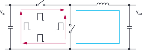
Figure 2. Different paths with different directions of current flow in a hot loop.
Figure 3 shows the real current loops on which the circuit is based. One current loop is shown in blue and another one is shown in green. Switching back and forth between these complete current loops does occur; in some paths, however, the currents flow in the same direction in both current loops, so they are superimposed to form a continuous current and thus are not critical as far as EMC is concerned. These traces are not referred to as hot loops.
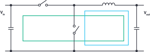
Figure 3. Real current loops leading to a so-called hot loop.
The hot loops in switching regulators differ depending on the switching regulator topology. They should be designed to be as narrow and compact as possible to minimize the noise generated as well as its transmission. The Silent Switcher 2 technology from Analog Devices makes the critical hot loops as small as possible through the integration of input capacitors in the IC package. Likewise, by splitting the hot loop into two symmetrical shapes, two magnetic fields of opposite polarities are created and the radiated noise cancels itself out to a great extent. An example of a switching regulator with this technology is the LT8609S from Power by Linear.
Author details: Frederik Dostal, Field Applications Engineer, Analog Devices
To contact Frederik Dostal use this email address - frederik.dostal@analog.com


