
This technology for creating a biodegradable silk fibroin film allows microfabrication with polymer or metal structures manufactured from photolithography. It can be a key technology in the implementation of silk fibroin-based biodegradable electronic devices or locaised drug delivery through silk fibroin patterns.
Silk fibroins are biocompatible, biodegradable, transparent, and flexible, which makes them excellent candidates for implantable biomedical devices, and they have also been used as biodegradable films and functional microstructures in biomedical applications. However, conventional microfabrication processes require strong etching solutions and solvents to modify the structure of silk fibroins.
To prevent the silk fibroin from being damaged during the process, Professor Hyunjoo J. Lee from the School of Electrical Engineering and her team came up with a novel process, named aluminum hard mask on silk fibroin (AMoS), which is capable of micropatterning multiple layers composed of both fibroin and inorganic materials, such as metal and dielectrics with high-precision microscale alignment. The AMoS process can make silk fibroin patterns on devices, or make patterns on silk fibroin thin films with other materials by using photolithography, which is a core technology in the current microfabrication process.
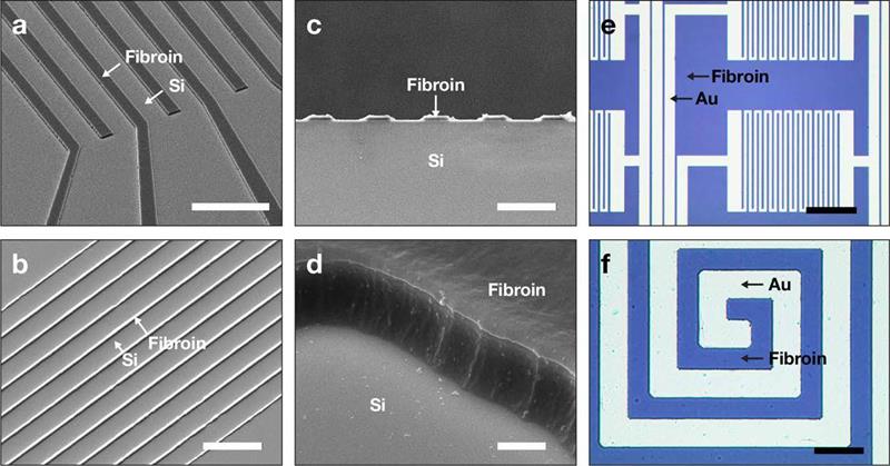
| Below: Fibroin microstructures and metal patterns on a fibroin produced by using the AMoS mask |
| Below: Biocompatibility assessment of the AMoS Process. Top: Schematics image of a) fibroin-coated silicon b) fibroin-pattered silicon and c) gold-patterned fibroin. Bottom: Representative confocal microscopy images of live (green) and dead (red) primary cortical neurons cultured on the substrates |
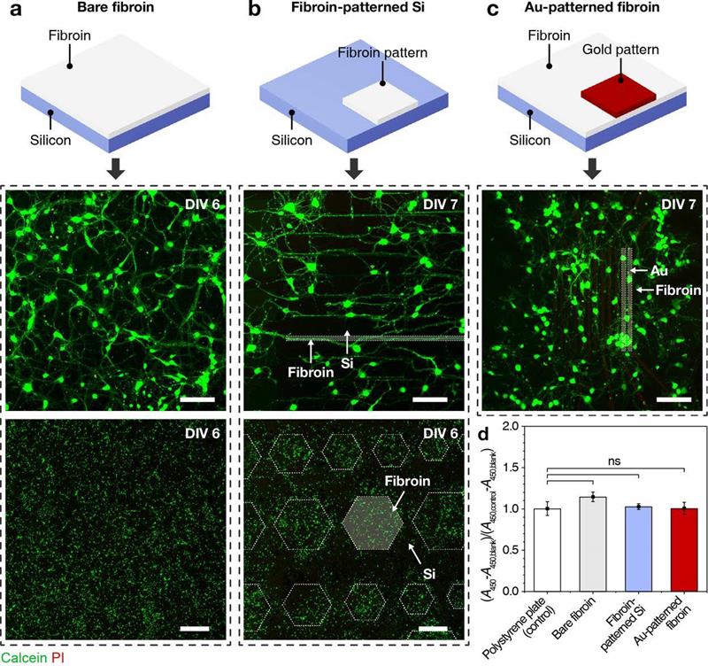
The team successfully cultured primary neurons on the processed silk fibroin micro-patterns, and confirmed that silk fibroin has excellent biocompatibility before and after the fabrication process and that it also can be applied to implanted biological devices.
Through this technology, the team realised the multilayer micropatterning of fibroin films on a silk fibroin substrate and fabricated a biodegradable microelectric circuit consisting of resistors and silk fibroin dielectric capacitors in a silicon wafer with large areas.
They also used this technology to position the micro-pattern of the silk fibroin thin film closer to the flexible polymer-based brain electrode, and confirmed the dye molecules mounted on the silk fibroin were transferred successfully from the micropatterns.
Prof Lee said, “This technology facilitates wafer-scale, large-area processing of sensitive materials. We expect it to be applied to a wide range of biomedical devices in the future. Using the silk fibroin with micro-patterned brain electrodes can open up many new possibilities in research on brain circuits by mounting drugs that restrict or promote brain cell activities.”


