
Solution-processable organic semiconductors are being highlighted for their potential application in printed electronics, becoming a feasible technique to fabricate large-area flexible thin film at a low cost. The field-effect mobility of small-molecule organic semiconductors is dependent on the crystallinity, crystal orientation, and crystal size. A variety of solution-based coating techniques, such as ink-jet printing, dip-coating, and solution shearing have been developed to control the crystallinity and crystal orientation, but a method for developing techniques to increase the crystal size of organic semiconductors is still needed.
Using their new developed technique, the researchers say the cystallisation process of organic semiconductors can be controlled precisely, and therefore large-area organic semiconductor thin film with controlled crystallinity can be fabricated.
A variety of solution-based coating techniques cannot control the fluid-flow of solutions appropriately, so the solvent evaporates randomly onto the substrate, which has difficulty in the fabrication of organic semiconductor thin film with a large crystal size.
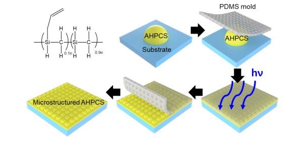
The research team integrated inorganic polymer microstructures into the solution shearing blade to solve this issue. The inorganic polymer can easily be microstructured via conventional moulding techniques, has high mechanical durability, and organic solvent resistance. Using the inorganic polymer-based microstructure blade, the research team controlled the size of small molecule organic semiconductors by tuning the shape and dimensions of the microstructure.
| Above: Chemical structure of inorganic polymer (AHPCS) and the fabrication process of a microstructured AHPCS shearing blade |
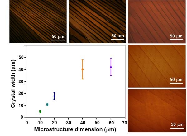
The microstructures in the blade induce the sharp curvature regions in the meniscus line that formed between the shearing blade and the substrate, and therefore, nucleation and crystal growth can be regulated. Hence, the research team fabricated organic semiconductor thin-film with large crystals, which increases the field-effect mobility.
The research team also demonstrated a solution shearing process on a curved surface by using a flexible inorganic polymer-based shearing blade, which expands the applicability of solution shearing.
Professor Steve Park of KAIST, said, “Our new solution shearing system can control the crystallisation process precisely during solvent evaporation.” He added, “This technique adds another key parameter that can be utilised to tune the property of thin films and opens up a wide variety of new applications.
| Above: The increasing trend of organic semiconductor crystal size with increasing the microstructure dimension |


