
Their work is expected to help semiconductor manufacturers to continue to innovate, producing smaller, faster, and more energy-efficient computer chips for computers and smartphones.
The processing speeds of processors used in electronic device has continued to accelerate as the number of transistors able to fit on a single computer chip is increased. To keep up with this pace of innovation, computer manufacturers are continually on the lookout for new methods to make each transistor ever smaller.
Current microprocessors are made by adding patterns of circuits to flat silicon wafers, but one way to cram more transistors in the same space is to fabricate 3D-structures. An example of which is fin-type field effect transistors (FETs) which have fin-like silicon structures that extend into the air, off the surface of the chip.
This method, however, requires a silicon crystal with a perfectly flat top and side-surfaces, instead of just the top surface, as with current devices. As a result designing these types of chips requires new knowledge of the atomic structures of the side-surfaces.
Researchers at Osaka University and the Nara Institute of Science and Technology report that they have used STM to image the side-surface of a silicon crystal for the first time. STM is a powerful technique that allows the locations of the individual silicon atoms to be seen. By passing a sharp tip very close to the sample, electrons can jump across the gap and create an electrical current. The microscope monitored this current, and determined the location of the atoms in the sample.
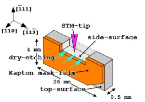 A schematic of a Si(110) sample with a Kapton film mask: dry etching from the (110) top-surface and STM-tip approaching to the (-111) side-surface.
“Our study is a big first step toward the atomically resolved evaluation of transistors designed to have 3D-shapes,” study co-author Azusa Hattori said.
To make the side-surfaces as smooth as possible, the researchers first treated the crystals with a process called reactive ion etching. Coauthor Hidekazu Tanaka said, “Our ability to directly look at the side-surfaces using STM proves that we can make artificial 3D structures with near-perfect atomic surface ordering.”
Main image: Spatial-derivative STM images with 200x200 nm^2 at Vs = +1.5 V. Flat terraces become brighter and edges darker. The downstairs direction runs from left ((110) top-surface) to right ((-1-10) back-surface). (Credit : Osaka University)


