
However, there are still some cases where a negative voltage is required, including:
- high performance/high speed A/D and D/A converters
- gallium nitride power transistor bias
- laser diode bias in optical modules
- LCD bias
Typically, these applications are powered by one or more positive supply rails with step-down converters and LDOs as point of load regulators. In most cases, the mains supply does not provide the negative voltage, which means it has to be generated from a positive rail.
There are a number of ways to generate a negative voltage, mainly dependent on the input voltage, output voltage and output current required. Examples include: inverting charge pumps; inverting buck-boost converters; and CUK converters. Each has its advantages and disadvantages.
Inverting charge pumps
Inverting charge pumps, which can be regulated or unregulated, are typically used for output currents of about 100mA. They follow a simple two step conversion principle and only require three capacitors.
- Charge a capacitor from a positive input voltage
- Discharge the capacitor to an output capacitor while reversing the connection, so the positive terminal is connected to the negative and vice versa.
This approach generates a negative voltage equal to the input voltage – for example, -5V from a +5V supply. The TPS60400 family is an example of such a device. The absolute value of the output voltage can only be equal to or smaller than the input voltage. So, if a lower absolute output voltage is required, an LDO can be added. The LM27761, which has an integrated LDO, is a suitable device whose output voltage can be adjusted from -1.5V to -5V from a 5.5V supply.
| Schematic of an inverting buck-boost converter |
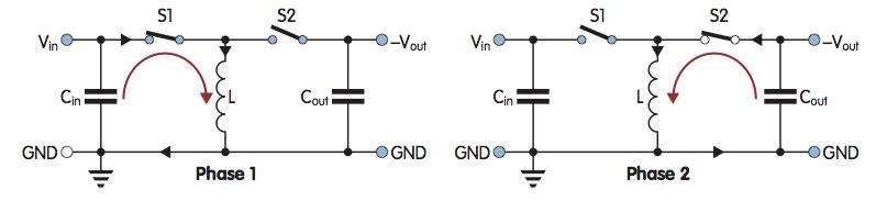
Inverting buck-boost converters
For larger output currents, inductive solutions – such as the inverting buck-boost converter – are used. These generate a negative output voltage which can be greater or smaller than the input voltage and provide an advantage over charge pumps.
In the first step, when S1 is closed, an inductor is charged with current. In the second step, S1 is opened and S2 is closed. The current in the inductor continues to flow in the same direction and charges the output negative. Typically, S2 can be implemented as an active switch, but is a diode in most cases.
The output voltage depends on the duty cycle (D). With:
D=Ton/T and ton.Vin=toff.|Vout|
The output voltage is defined as
|Vout|=Vin.[D/(1-D)]
In figure 1, input current only flows when S1 is closed and the output capacitor is only charged when S2 is closed. Therefore, the input and output currents are discontinuous and the peak inductor current is much larger than the average output current. The topology has a low loop bandwidth because a delay in the system’s response sets a limit for the control loop bandwidth. If the system demands higher current, the duty cycle has to be increased, which means a shorter toff. This decreases the amount of current transferred to the output in that switching cycle, so the output voltage drops even further. The control loop therefore needs time until the inductor current in the ton phase rises to the level where there is a higher current in the shorter toff phase delivered to the output. This effect, referred to as right half plane zero, makes the response of the control loop somewhat slow. The loop bandwidth of an inverting buck-boost converter is typically in the order of 10kHz.
| Schematic of an inverting buck converter |
CUK converter
A CUK converter combines a boost converter with a step-down converter, with the two stages coupled by a capacitor. This topology requires two inductors or one coupled inductor, but supports continuous input and output current and therefore offers advantages for systems that demand low input and output voltage ripple. The control loop bandwidth, and therefore its speed, is lower than the inverting buck-boost converter.
For applications that require low 1/f noise in frequencies ranging to 100kHz, the CUK or the inverting buck-boost converter are not optimal solutions because their control loop bandwidth is much less than 100kHz. A solution to this issue is the inverting buck converter.
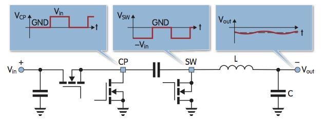
Inverting buck converter
Replacing the input inductor of the CUK converter with a high side switch leads to a new topology; the inverting buck converter. This consists of a charge pump inverter followed by a step-down converter and requires only one inductor. The control loop regulates the output voltage of the step-down converter and, because the charge pump stage is combined with the step-down converter’s power stage, it runs with the inverse of the step-down converter’s duty cycle.
In figure 2, the voltage at CP is switching between VIN and GND while the voltage on SW is between –VIN and GND. As the charge pump stage does not boost the input voltage, the voltage across the internal switches is only VIN, so lower than in the inverting buck-boost or CUK converter. This means more efficient low voltage switches can be used. The output LC of the buck-stage filters the output voltage so output voltage ripple becomes very small.
The TPS63710 offers several advantages over classical topologies, including:
- a control loop bandwidth of about 100kHz gives fast transient response
- continuous output current for low output voltage ripple
- low gain in the gain stage, so the noise level is not increased after the noise filter by a high gain of the gain stage
- a low 1/f noise reference system
The voltage of a bandgap (VBG) is amplified and inverted to generate a negative reference voltage on VREF using an external voltage divider formed by R1 and R2. This reference voltage is set to a voltage slightly less than (in absolute value) the output voltage. This voltage is filtered by an RC filter consisting of an internal 100kΩ resistor and an external capacitor (CCAP) for low 1/f noise up to 100kHz. The gain stage is formed by an inverter combined with a step-down converter with a voltage gain of 1/0.9.
In most converters, the voltage divider to set the output voltage is on the output side between VOUT and GND, which sets a certain gain of the output stage of VOUT / VREF. This increases 1/f noise on the reference voltage. In TPS63710, the gain is 1/0.9, which keeps 1/f noise at nearly the same level as the reference voltage on CCAP.
The TPS63710 accepts inputs ranging from 3.1 to 14V, with an output voltage ranging from -1V to -5.5V. As the TPS63710 uses a buck topology, the input voltage, in absolute value, needs to be larger than the output voltage by a factor of 1/0.7 at least.
Figure 3 shows the schematic of an inverting buck converter optimised for a typical 5V input voltage generating a -1.8V supply at up to 1A. Small size ceramic capacitors used on the input, the CP pin and the output have small electrical series resistance and therefore provide lowest output voltage ripple.
TPS63710 provides the highest efficiency of comparable solutions. The QFN package with thermal pad provides a low thermal resistance to the pcb. This keeps the junction temperature low, even when the device is
Capable of operating in high ambient temperatures, the TPS63710 provides:
- A 1/f noise of ~30mVRMS
- A full power efficiency of more than 86%
- An output voltage ripple of less than 10mVpp
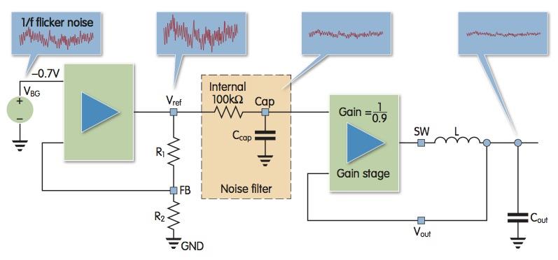
| Block diagram of the principle behind the TPS63710 |


