
For output voltages exceeding the ±5V range, additional circuitry is necessary, which results in a quite bulky and expensive bias supply solution. However, it is possible to create a low cost LCD bias supply solution using only one integrated boost converter to generate all necessary bias voltages.
The input voltage for this automotive application ranges from 3V up to 13.2V. Table 1 shows a typical bias supply specification for a 12in display. The 6.6V and +6.6V rails have tolerances of ±1.5%, which means good regulation is necessary. The two other voltages have much larger tolerance bands, with at least 20% deviation from the nominal voltage. Meanwhile, the current demands are quite different with around 50mA for the tight tolerance outputs and less than 1mA for the gate drive voltages.
At first glance, the current and power demands make a charge-pump based solution feasible, which is usually also attractive from a cost point. On closer investigation, it becomes clear that integrated charge-pump devices are limited to voltages around ±5V on the input as well on the output and therefore not applicable for this design.
A solution based on standard switch mode topologies could also be considered, but this will not only be too bulky, but will also be too expensive.
The negative voltages could also be generated by an inverting buck-boost – the 14V by a boost, while the 6.6V rail needs a topology which can work in buck and boost mode as the input can be higher and lower than the output. This would require four converters and four inductors in total.
A suitable means of generating the 6.6V required in this application is a Sepic converter, which can work in buck as well in boost mode. The Sepic converter uses a flyback topology, in which the output winding is clamped to the primary by a capacitor. This reduces the overshoot and high spikes at the switching node for which a flyback design is infamous.
Like a flyback converter, the Sepic can also have several output windings, if coupled inductors, rather than individual inductorsm are used. The four voltages are either quite similar even if negative or a multiple of another voltage in the system. So a coupled inductor with several windings should enable a designwhich needs only such an inductor and a single integrated boost converter.
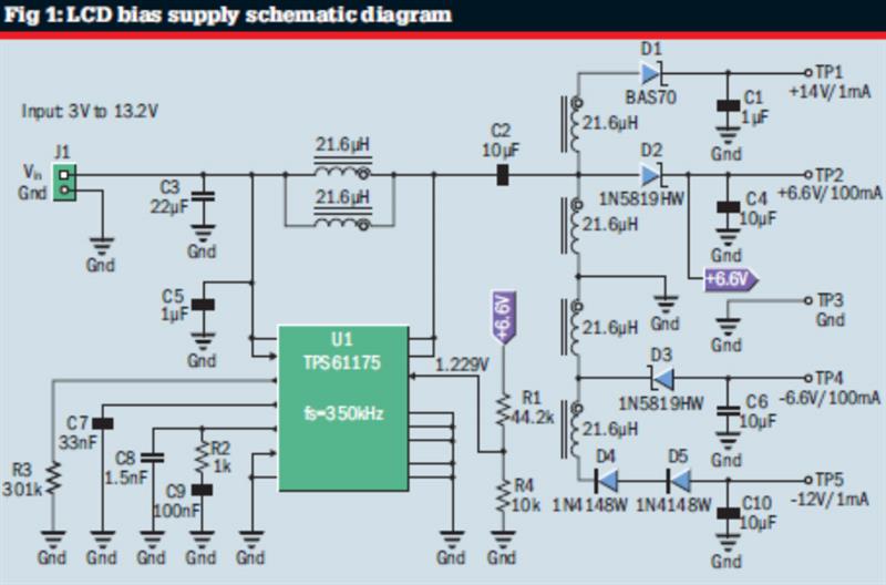
Wuerth's WE-FLEX flyback transformers offer six equal windings on one core. By putting them in parallel or series and stacking them accordingly, all voltages can be generated by such a single magnetic. Figure 1 shows the built and tested circuit, which uses a transformer with a base inductance of 21.6µH and a TPS61175 boost converter working at a switching frequency of 350kHz.
The input to the power stage, as well as the output 6.6V rail, is designed like a normal Sepic converter. Two windings in parallel on the input provide the required inductance and the inductor on the output is connected between ground and the coupling capacitor on the switching node. The output of this rail is connected to the feedback of the controller, which results in an accuracy which meets the specification of ±1.5%. All other windings are stacked onto this winding, as is often seen on flyback converters without direct connection to the coupling capacitor.
Compared to the 6.6V output, no power is transferred from the input to the output via the coupling capacitor, but all power needs to be transferred by magnetic coupling between the additional windings. For good cross regulation between the outputs, good coupling is mandatory.
By dismantling the WE-FLEX transformer, it was discovered the part features three inner windings and three outer windings on the bobbin. For this power supply, it is connected in such a way that the 6.6V and -6.6V windings are inside, with one primary inductor on the side and the second one on the top to achieve good coupling and therefore good output voltage accuracy for the negative rail (see fig 2).
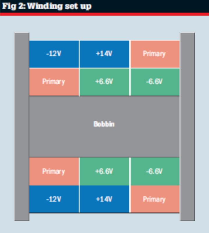
The two remaining outside windings are used for the 14V and -12V outputs, which allow much higher tolerances. By selection of the rectifier diodes, the output voltage is fine tuned to meet the specified values.
Although the output power is quite low at around 750mW, high efficiency is achieved over the entire input voltage range. With a 3V input, the efficiency is 87%, at 6.3V, it is 89% and at the maximum input voltage of 13.2V, efficiency is 85%.
Cross regulation
The more important measurement is the cross regulation between all four outputs with the maximum load.
All output voltages are well regulated and within their tolerances. Due to the peak detection of the flyback rectifier, this multi output Sepic converter will not work properly if an output is not loaded at all, especially if another output is fully loaded. This is not critical in this application, because a certain load is always connected to all four outputs. In applications where this is not the case, a resistor which only draws a little current has to be connected on each output to avoid the output voltage rising too high, which could damage the components or subsequent circuits. For good cross regulation, the rail with the highest load should always be controlled directly by the feedback of the converter.
The switching node of the Sepic converter with stacked flyback windings shows a smooth waveform without large spikes due to the clamping capacitor (C2 on the schematic). This reduces the overall EMI heavily and has also a positive impact on the efficiency as no additional snubber network is needed.
A Sepic converter can be easily extended to multiple outputs by stacking additional windings on the output inductance. This approach combines several advantages of a flyback like multi-output capability and buck-boost operation without the disadvantage of large spikes on the switching node caused by the leakage inductance of the coupled inductor. A standard transformer from stock with six identical windings is connected in such a way to generated four different output voltages, positive as well as negative, with only one integrated boost converter. This results in a small and cost effective solution for a LCD bias supply with wide input voltage range.
Author profiles:
Bernd Geck heads TI's European Power Supply Design Services Team.
Matthias Ulmann is a reference design engineer in TI's EMEA Design Services Group.
Information on this circuit – including schematics, layout and bill of material – is available by searching for PMP10051 on TI's Reference Design Library (www.ti.com).


