
One challenge in stacking ICs is to retain a high compound yield and to not include faulty dice. This requires testing the dice before stacking them; for example, through the interconnect microbumps.
However, many engineers have considered it impossible to probe these microbumps because the arrays are too large and the microbump pitch of less than 40µm is too small.
In response, nanoelectronics research centre imec has used National Instruments’ Semiconductor Test System (STS) to develop a fully automated system to characterise prototype probe cards for large-array, fine-pitch microbumps on advanced test wafers.
Probing microbumps
Due to its high-precision, 3D-SIC manufacturing is prone to defects and every IC needs to undergo electrical tests to weed out defective parts and guarantee product quality. 3D-SICs, which typically contain complex die designs in advanced technology nodes, need to be tested using advanced test and design-for-test approaches.
A number of test challenges are unique to the stacking process itself. One is testing dies prior to stacking; essential to obtain acceptable compound stack yields and to not lose good dice in a stack with one faulty die.
The non-bottom dies of the stacks have their functional access exclusively through large arrays of fine-pitch microbumps, which are too dense for conventional probe technology.
A common approach is to equip these dice with dedicated pre-bond probe pads. However, this comes with drawbacks, such as increased silicon area and test application time and a reduced interconnect performance. To avoid these drawbacks, imec and its partners set out to enable probing directly on the microbumps, a task previously thought impossible.
Fully automatic test system to evaluate microbump probing
The probe challenges for this type of microbump array include:
- Providing a test system with a sufficient number of channels for large arrays of microbumps. Test systems with 1200 channels are usually expensive and a soft-docking cable interface with that many channels would be nearly impossible to connect and maintain.
- Landing with all probe tips on the microbumps. Advanced probe cards are non-see-through, they require an advanced probe station that determines probe-tip landing locations using software overlay of microbump images from a downward-looking camera and images of the probe tips from an upward-looking camera. Sufficient positioning accuracy is required from both the probe tips with regard to each other, as well as from the probe station while stepping over the various dice on the wafer.
- Establishing a proper electrical contact between probe tip and microbump. The quality of the probe contact is expressed by the contact resistance (Rc). This not also depends on the metallurgy of the microbumps and the shape and material of the probe tips, but also on the force with which the probe station presses the wafer against the probe tips (over-travel) and the cleanliness of the probe tips. Hence, while operating the probe station, we need to carefully consider the over-travel of the wafer chuck.
- Probe marks should not negatively impact the stack’s interconnect yield. The prime function of microbumps is to form a reliable electrical connection between two stacked dice. Marks should not deteriorate the interconnect stacking yield and probe marks should be limited in topology, or be erasable through a reflow process.
- The approach should be economically feasible. Pre-bond test is constrained by cost: it should not cost more to perform the test than to skip it.
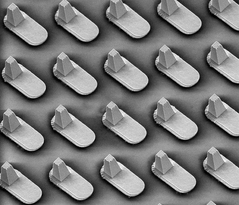
To address these challenges, imec worked with probe card supplier Cascade Microtech, which provided prototypes of its advanced Pyramid Rocking Beam Interposer (RBI) probe cards. These probe cards contain an IC design specific probe core, which includes a thin film with MEMS-type probe tips. Cascade’s probe cores support more than 1200 core I/Os, sufficient for WIO1 (JEDEC’s JESD-229 standard for Wide I/O single data rate DRAM). The RBI probe tips require less than 1gf/tip to make proper electrical contact and the heel of the tip makes physical contact with the wafer (pictured right) in such a way that the probe mark is typically only 6 × 1µm.
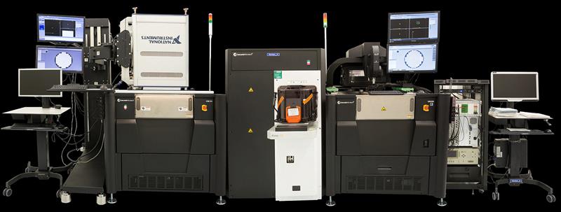
To prove the feasibility of microbump probing with these probe cards, imec built a fully automatic test system consisting of a dual CM300 probe station from Cascade Microtech, a hard-docking STS test head with PXI test instruments from NI, a test head manipulator from Reid-Ashman and test programme and data analysis software based on LabVIEW and developed at imec.
The NI STS test head contains two PXI racks with test instruments. Rack 1 holds instruments for parametric and functional tests, while rack 2 is dedicated to microbump probing and contains a PXI-4072 digital multimeter connected to an ultra-wide switch matrix with nine concatenated PXIe-2535 modules, each with 136 output columns. This made it possible to connect each of the four DMM channels under software control to any of the 1224 SMX output columns.
The system supports two- and four-point Kelvin resistance measurements between any pair of probe tips – for daisy chains – as well as between a single probe tip and all other probe tips ganged, for characterisation of that single probe tip when all probe tips are shorted through the probed wafer.
Conclusion
Tests in 300mm wafers designed and manufactured in-house by imec and featuring microbumps with various metallurgies, pitches, diameters and sizes), demonstrated that all WIO1 probe tips landed on the corresponding microbumps; the actual contact resistance between probe tip and microbump was approximately 0.1Ω. However, the resistance of the trace through the thin film membrane on the probe core is often included in the measurement and this is approximately 5Ω.
The probe marks on the Cu were small and, while the probe marks on Sn were larger, they could be removed through reflow. Imec also demonstrated there were no stacking interconnect yield differences between all four cases of bottom/top microbumps probed/not-probed.
Through cost modelling, it was possible to demonstrate that, for single-site testing, the Pyramid Probe cards, although expensive, outperformed pre-bond testing through dedicated probe pads financially.
Crucially, the work showed that microbump probing was technically and economically feasible.
Author profile
Ferenc Fodor is a test development engineer with imec
| Benefits working with NI products • NI’ STS hard-docking test head enabled imec to make more than 1200 instrument-to-probe connections, something not possible with a manual cable interface. • The PXIe-2535 switch matrix modules allowed concatenation of an ultra-wide switch matrix with an unlimited lifetime of FET switches. Its unlimited simultaneous cross-point connection provided the ability to perform probe checks. • The test times were short; about 100 two-point resistor measurements per second. • LabVIEW provided an easy-to-program interface to the system. |


